Method for creating thick oxide on the bottom surface of a trench structure in silicon

a trench structure and silicon technology, applied in the field of trench transistors, can solve problems such as low efficiency

Inactive Publication Date: 2005-03-01
SEMICON COMPONENTS IND LLC
View PDF17 Cites 38 Cited by
  • Summary
  • Abstract
  • Description
  • Claims
  • Application Information

AI Technical Summary

Benefits of technology

The present invention provides a trench metal oxide semiconductor field effect transistor (MOSFET) having a dielectric layer that is t...

Problems solved by technology

However a uniformly thicker gate dielectric layer req...

Method used


Image

  • Method for creating thick oxide on the bottom surface of a trench structure in silicon
  • Method for creating thick oxide on the bottom surface of a trench structure in silicon
  • Method for creating thick oxide on the bottom surface of a trench structure in silicon

Examples


Embodiment Construction

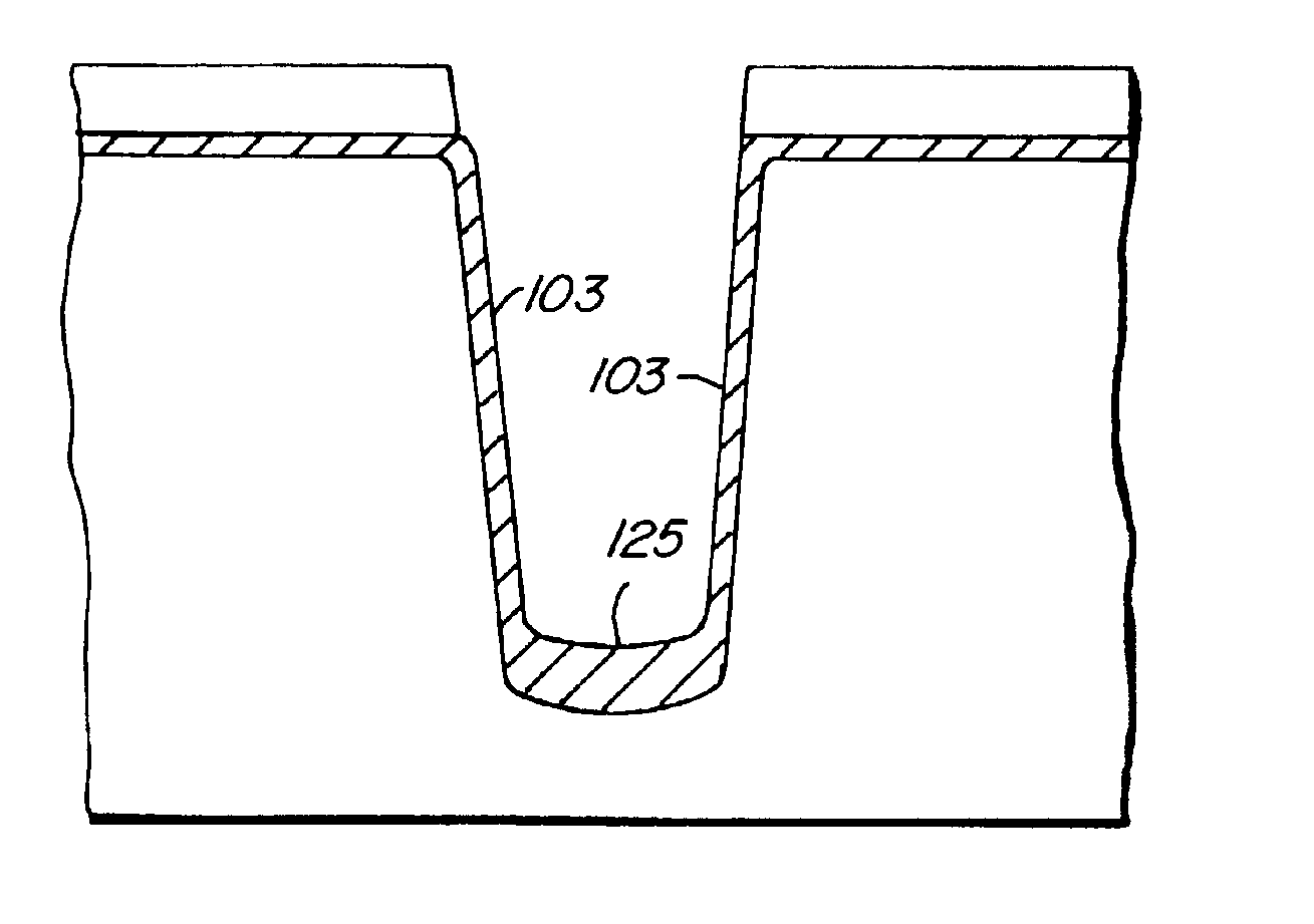
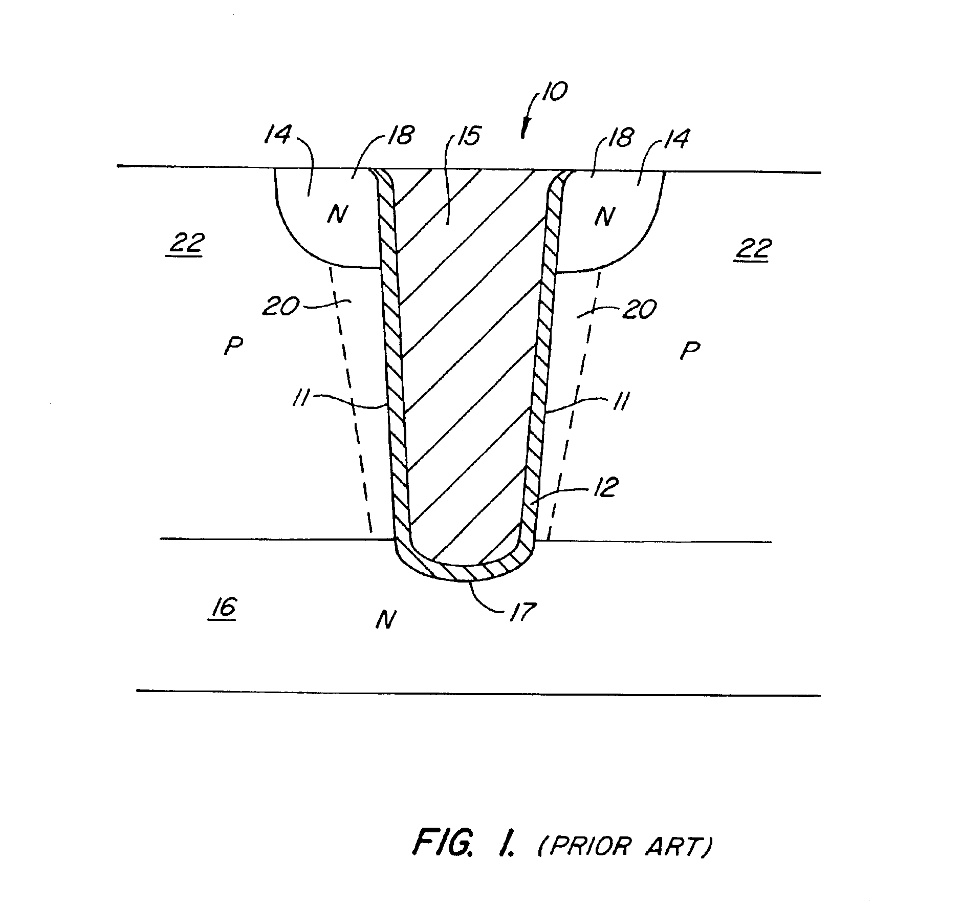
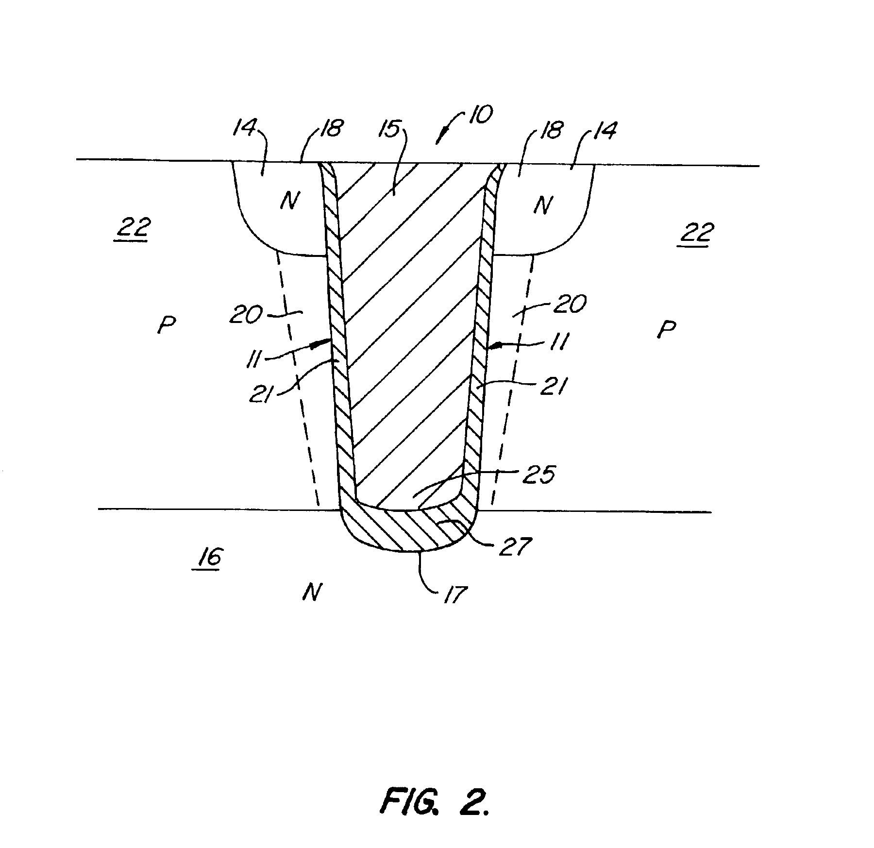
FIG. 2 illustrates an exemplary n-type trench transistor with a superior gate isolation structure according to an embodiment of the present invention. A trench 10 with sidewalls 11 and a bottom 17 extends into a silicon substrate body region 22. The source electrode is shown in FIG. 2 as being two N-type regions 14 adjacent to and on opposite sides of the trench 10. The drain electrode is shown as an N-type region 16 below a P-type body region 22. It is to be understood that in the case of a p-type transistor, the conductivity type of each of the drain, source and body regions may be reversed. A conductive material forms the gate 15 of the trench transistor. The gate 15 may extend above, below, or at the level of the top surface of the silicon substrate body region 22. In operation, drain region 16 may be electrically contacted through the substrate of the device, the gate 15 may be electrically contacted via a conductive layer (e.g., aluminum) above the transistor (not shown), and ...


PUM


Abstract

A gate isolation structure of a semiconductor device and method of making the same provides a trench in a silicon substrate, wherein a dielectric layer is formed on sidewalls and bottom of the trench, the dielectric layer having a first thickness on the sidewalls and a second thickness at the bottom that is greater than the first thickness. The thicker dielectric layer at the bottom substantially reduces gate charge to reduce the Miller Capacitance effect, thereby increasing the efficiency of the semiconductor device and prolonging its life.

Description

CROSS REFERENCES TO RELATED APPLICATIONSA first related application, filed concurrently with the present application, is U.S. patent application Ser. No. 09 / 640,955, in the names of Izak Bencuya et al. and entitled “Vertical MOSFET with Ultra-Low Resistance and Low Gate Charge” and assigned to the present assignee. A second related application, filed concurrently with the present application, is U.S. patent application Ser. No. 09 / 640,496 now U.S. Pat. No. 6,444,528, in the name of James J. Murphy, and entitled “Selective Oxide Deposition in the Bottom of a Trench” and assigned to the present assignee. Both of these applications are incorporated by reference herein for all purposes.BACKGROUND OF THE INVENTIONThe present invention relates in general to field effect transistors, and in particular to trench transistors and methods of their manufacture.FIG. 1 is a simplified cross-section of a portion of a conventional trench power metal-oxide-semiconductor field-effect transistor (MOSF...

Claims


Application Information

Patent Timeline
IPC IPC(8): H01L21/00H01L21/02H01L29/66H01L21/336H01L29/768H01L29/78H01L27/108H01L31/062H01L29/76H01L31/06H01L29/423
CPCH01L29/42368H01L29/66666H01L29/7813H01L29/66734H01L29/7827
Inventor HURST, HENRY W.MURPHY, JAMES J.
Owner SEMICON COMPONENTS IND LLC
Why Eureka
Try Eureka