Method of fabricating trench isolation structures for integrated circuits using atomic layer deposition

a technology of atomic layer deposition and trench isolation, applied in the direction of semiconductor/solid-state device manufacturing, basic electric elements, electric devices, etc., can solve the problems of locos isolation, reducing resolution, and increasing difficulty in device isolation, which is critical to proper circuit operation

Inactive Publication Date: 2005-03-01
ASM INTERNATIONAL
View PDF5 Cites 87 Cited by
  • Summary
  • Abstract
  • Description
  • Claims
  • Application Information

AI Technical Summary

Problems solved by technology

Device isolation, which is critical to proper circuit operation, has become progressively more challenging.
In spite of its success, several limitations of LOCOS technology have driven the development of alternative isolation structures.
A well-known limitation in LOCOS isolation is oxide undergrowth at the edge of the hard mask (typically made of silicon nitride) that protects the active regions of the substrate during oxidation.
This so-called “bird's beak” poses a limitation to device density since it widens the isolation region, thereby reducing resolution, while causing stress within the substrate.
Another problem associated with the LOCOS process is its non-planarity.
For submicron devices, non-planarity becomes an important issue, often posing problems for photolithography and subsequent layer conformality.
The basic trench isolation process is, however, subject to drawbacks, including void formation in the trench during dielectric refill.
Such voids compromise device isolation as well as the overall structural integrity of the integrated circuit.
Unfortunately, preventing void formation during trench refill often places minimum size constraints on the trenches themselves, which can limit device packing density or the effectiveness of the device isolation.
A principal trade off in decreasing the trench depth is reducing the effectiveness of the device isolation, while the larger top openings of trenches with tapering sidewalls use up additional and valuable integrated circuit real estate.

Method used


Image

  • Method of fabricating trench isolation structures for integrated circuits using atomic layer deposition
  • Method of fabricating trench isolation structures for integrated circuits using atomic layer deposition
  • Method of fabricating trench isolation structures for integrated circuits using atomic layer deposition

Examples


Embodiment Construction

of deposition.

[0026]FIG. 8 is a schematic cross-section of a partially fabricated integrated circuit, illustrating a filled trench.

[0027]FIG. 9 is a schematic cross-section of a partially fabricated integrated circuit, illustrating the filled trench of FIG. 8 after planarization.

[0028]FIG. 10 is an equilibrium phase diagram for silicon oxide (silica) and aluminum oxide (alumina).

[0029]FIG. 11 is a plot of coefficient of thermal expansion as a function of weight percent Al2O3 in an Al2O3 / SiO2 mixture.

DETAILED DESCRIPTION OF THE PREFERRED EMBODIMENT

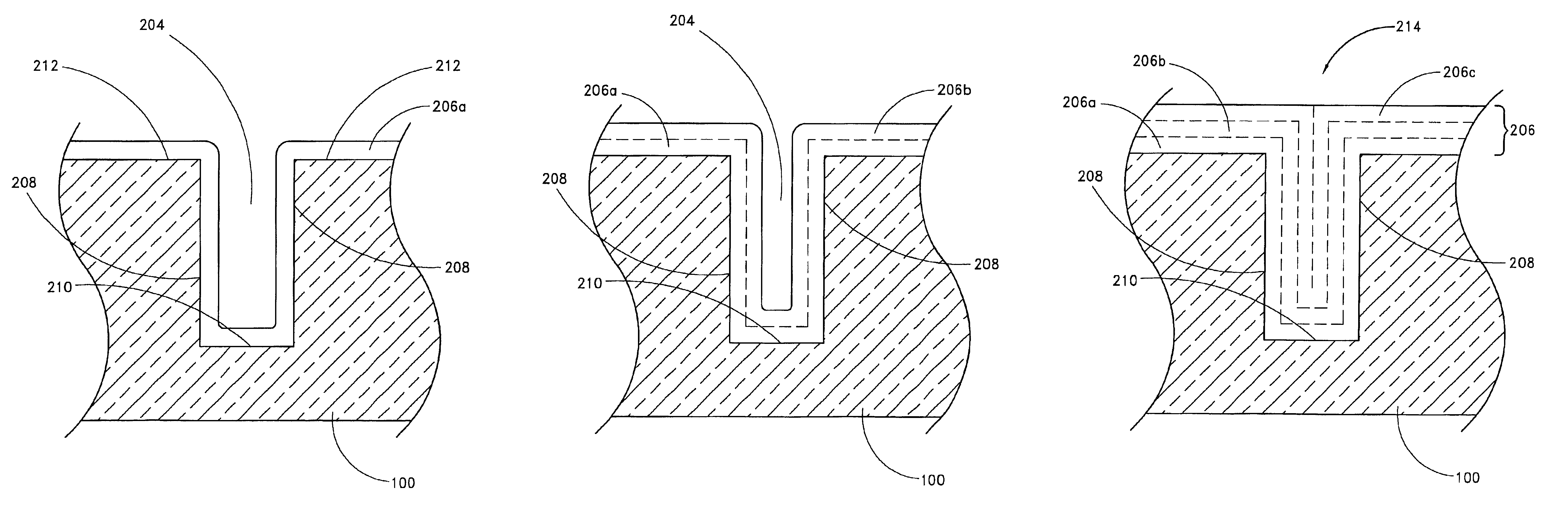
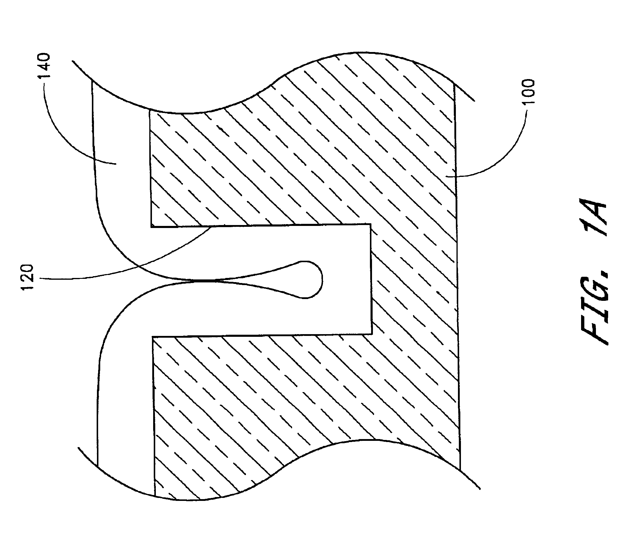
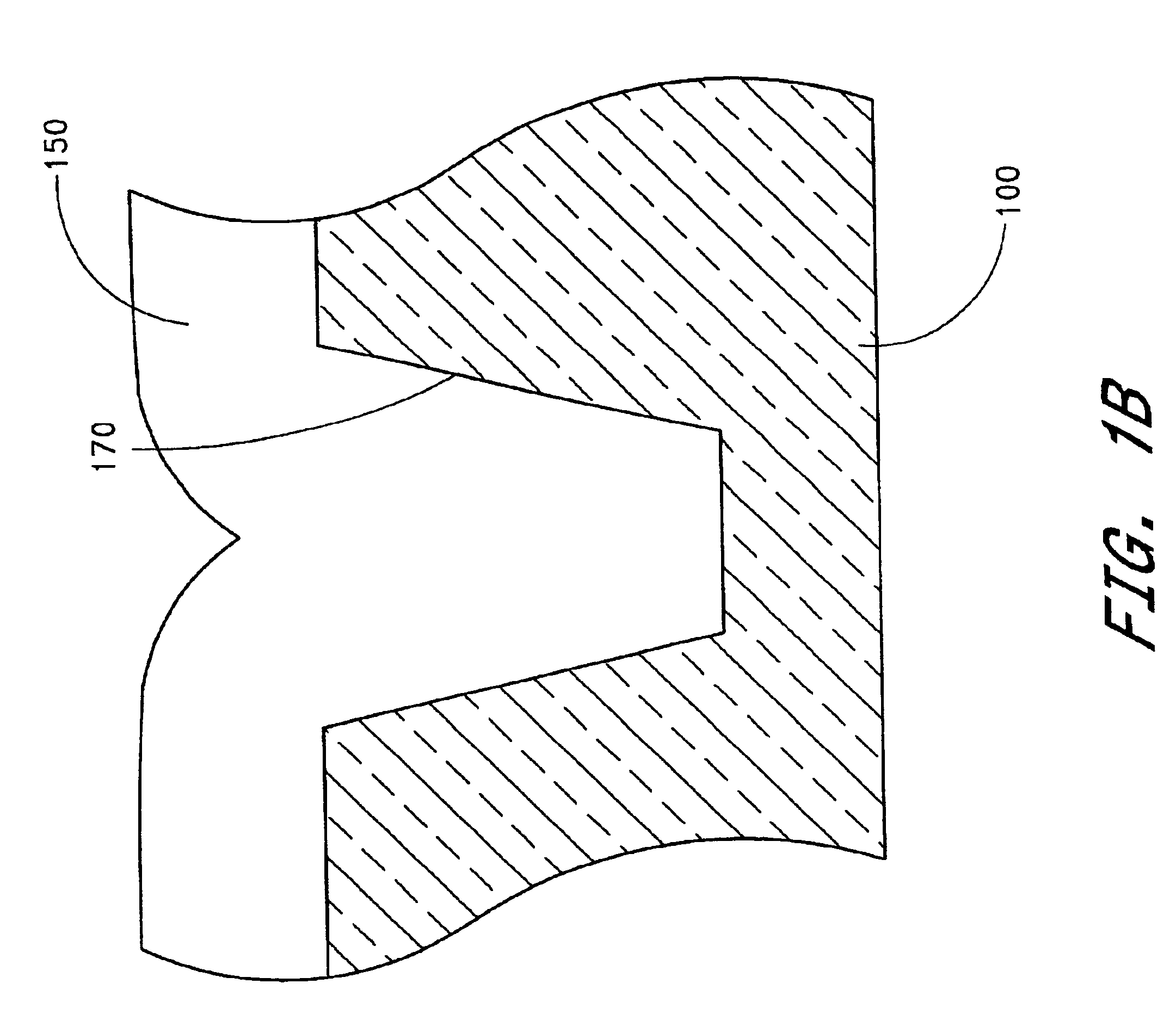
[0030]Although described in the context of trench isolation structures in integrated circuits, the skilled artisan will readily find application for the principles disclosed herein in a number of other contexts. The processes and structures of the preferred embodiments have particular utility where extremely thin layers are desired, particularly within openings that are narrow and deep.

[0031]As noted in the Background section above, the tre...


PUM

PropertyMeasurementUnit
pressureaaaaaaaaaa
pressureaaaaaaaaaa
pressureaaaaaaaaaa

Abstract

A dielectric film is formed by atomic layer deposition to conformally fill a narrow, deep trench for device isolation. The method of the illustrated embodiments includes alternately pulsing vapor-phase reactants in a string of cycles, where each cycle deposits no more than about a monolayer of material, capable of completely filling high aspect ratio trenches. Additionally, the trench-fill material composition can be tailored by processes described herein, particularly to match the coefficient of thermal expansion (CTE) to that of the surrounding substrate within which the trench is formed. Mixed phases of mullite and silica have been found to meet the goals of device isolation and matched CTE. The described process includes mixing atomic layer deposition cycles of aluminum oxide and silicon oxide in ratios selected to achieve the desired composition of the isolation material, namely on the order of 30% alumina and 70% silicon oxide by weight.

Description

FIELD OF THE INVENTION[0002]The invention relates generally to integrated circuit design and process technology. In particular, the invention pertains to a trench isolation structure and a method for filling isolation trenches.BACKGROUND OF THE INVENTION[0003]In silicon integrated circuit technology, a large number of isolated devices are fabricated on the same semiconductor substrate. Subsequently these devices are interconnected along specific paths to create the desired circuit configuration. In the continuing trend toward higher densities, devices are placed closer together with smaller spaces between them. Device isolation, which is critical to proper circuit operation, has become progressively more challenging.[0004]Over the last few decades a variety of isolation technologies have been developed to address the requirements of various integrated circuit types. In general, the various isolation technologies are different with respect to characteristics such as minimum isolation...

Claims


Application Information

Patent Timeline
Patent Type & Authority Patents(United States)
IPC IPC(8): H01L21/762H01L21/70H01L21/02H01L21/316
CPCH01L21/02145H01L21/02164H01L21/02178H01L21/02216H01L21/0228H01L21/76224H01L21/3144H01L21/3145H01L21/31612H01L21/3162H01L21/3141
Inventor RAAIJMAKERS, IVOSOININEN, PEKKA T.GRANNEMAN, ERNST H. A.
Owner ASM INTERNATIONAL
Why Eureka
Try Eureka