Method of fabricating semiconductor device

a semiconductor device and manufacturing method technology, applied in the field of mos transistors, can solve the problems of aggravated short-channel effects, degraded subthreshold characteristics, and low driving force of mos transistors, and achieve the effect of large driving for

Inactive Publication Date: 2005-03-01
PANASONIC CORP
View PDF21 Cites 10 Cited by
  • Summary
  • Abstract
  • Description
  • Claims
  • Application Information

AI Technical Summary

Benefits of technology

It is therefore an object of the present invention to provide a method of fabricating a semiconductor device with a large driving force, such as a MIS transistor, while suppressing downward penetration of an impurity from a gate insulating film of the MIS transistor having a gate electrode doped with the impurity.

Problems solved by technology

This causes the disadvantages of a lower driving force of the p-channel MOS transistor, degraded subthreshold characteristics, and aggravated short-channel effects.
However, as the gate length of a transistor becomes shorter with the increasing miniaturization and higher integration of a CMOS device currently pursued, a gate insulating film is also reduced in thickness to provide a sufficient driving force despite a reduction in voltage, which has caused the problem that a transistor with a sufficient driving force is not provided even if the gate insulating film is composed of a silicon oxynitride film.

Method used


Image

  • Method of fabricating semiconductor device
  • Method of fabricating semiconductor device
  • Method of fabricating semiconductor device

Examples


Embodiment Construction

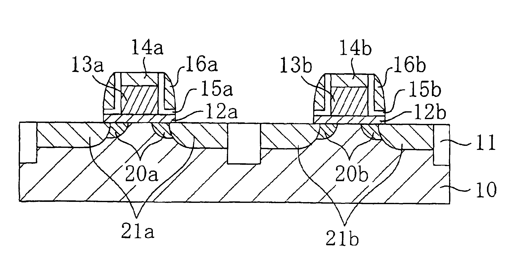
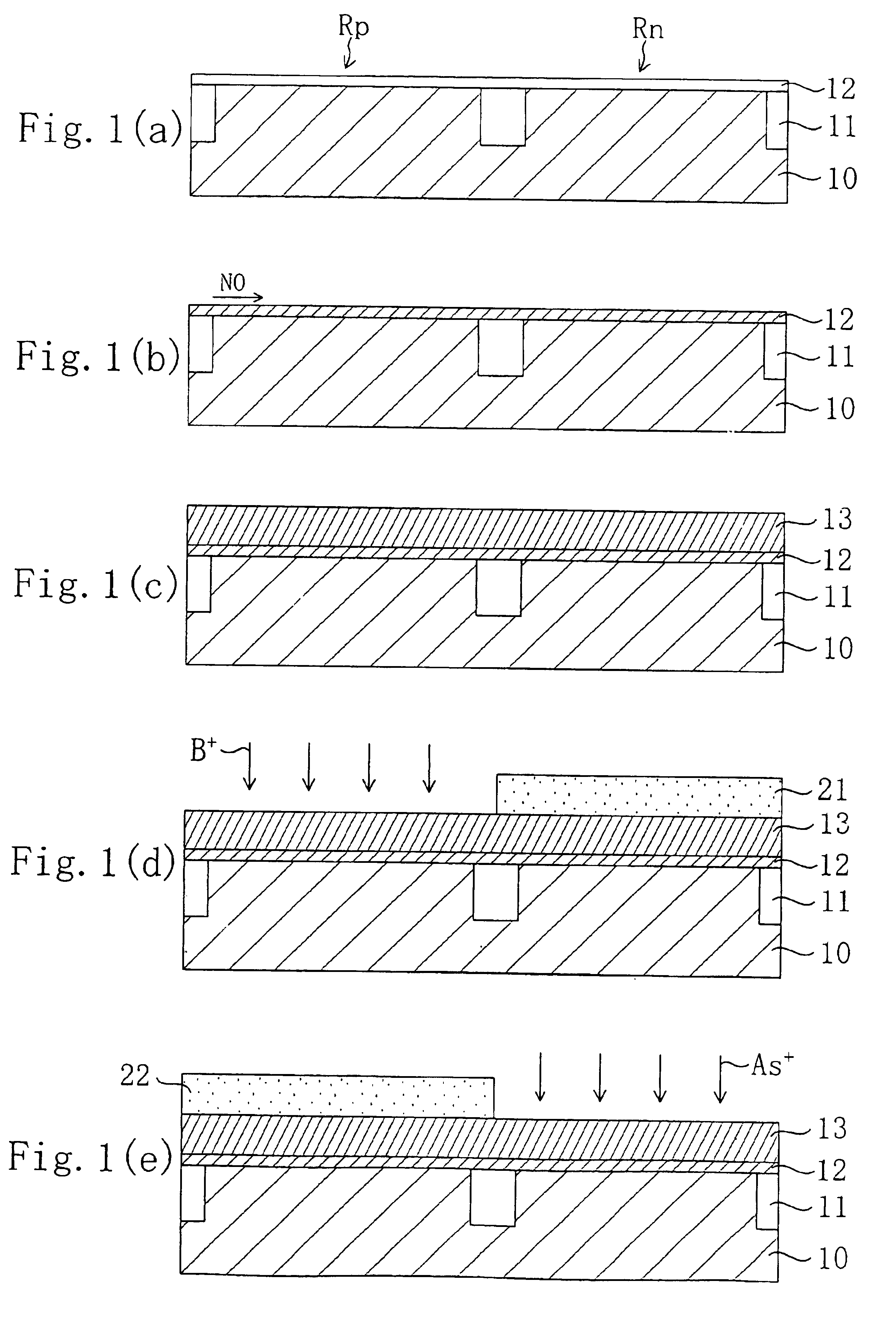
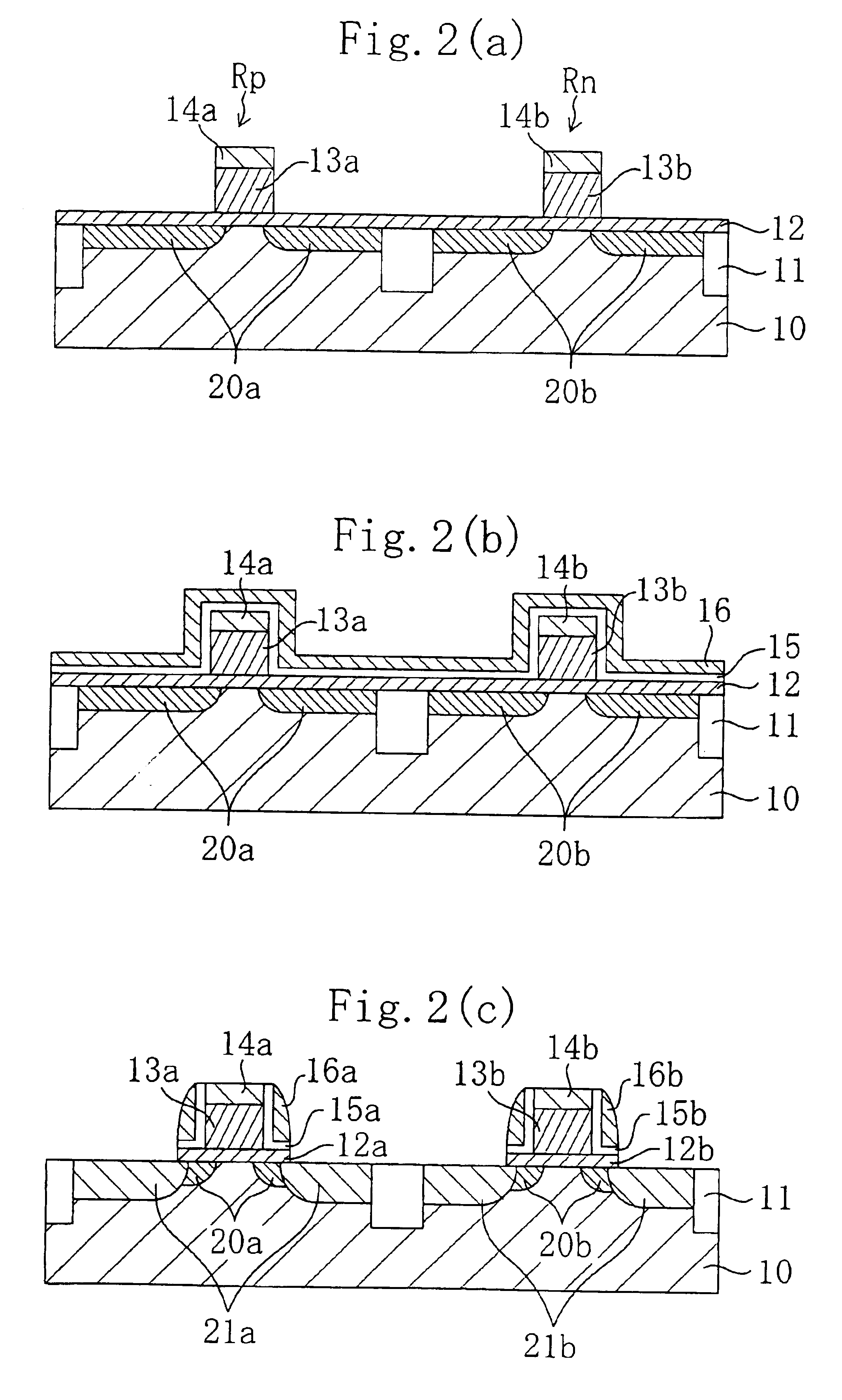
FIGS. 1(a) to (e) and FIGS. 2(a) to (c) are cross-sectional views illustrating the process of fabricating a semiconductor device (CMOS device) according to an embodiment of the present invention. Throughout the drawings, Rp denotes a region in which a p-channel MIS transistor is to be formed and Rn denotes a region in which an n-channel MIS transistor is to be formed.

In the step shown in FIG. 1(a), trench isolation regions 11 surrounding the p-channel MIS transistor formation region Rp and the n-channel MIS transistor formation region Rn are formed in a Si substrate 10. Then, the Si substrate 10 is kept in contact with an N2O gas at a temperature of about 1000° C. for about 60 sec, whereby a silicon oxynitride film 12 with a thickness of 2.8 nm is formed on the substrate 10.

It is to be noted that the method of forming the silicon oxynitride film is not limited thereto. For example, it is also possible to perform a heat treatment at about 1000° C., while keeping the surface of the Si...


PUM

PropertyMeasurementUnit
thicknessaaaaaaaaaa
temperatureaaaaaaaaaa
thicknessaaaaaaaaaa

Abstract

A silicon oxynitride film is formed on a substrate. Then, a heat treatment is performed, while keeping a surface of the silicon oxynitride film in contact with a gas containing nitrogen, such as an NO gas, to introduce at least nitrogen into the silicon oxynitride film and produce a steeply sloped distribution of nitrogen. A semiconductor film containing an impurity, such as an amorphous silicon film, is formed on the silicon oxynitride film. By forming a CMOS device with, in particular, a dual gate structure which comprises p-type and n-type MIS transistors each having a gate oxide film composed of the silicon oxynitride film and a gate electrode composed of a polysilicon film, a high driving force is provided, while boron penetration in the p-type MIS transistor is suppressed.

Description

BACKGROUND OF THE INVENTIONThe present invention relates to a MIS transistor having a polysilicon gate electrode provided on a gate insulating film and, more particularly, to an improvement in the driving force thereof.Doping of the gate electrode of a MOS transistor with an impurity has been performed conventionally and commonly to reduce the resistance of the gate electrode and thereby improve the driving force of the MOS transistor. In particular, a CMOS device typically has a so-called dual gate structure in which the gate electrode of an n-channel MOS transistor is doped with an n-type impurity (phosphorus or arsenic) and the gate electrode of a p-channel MOS transistor is doped with a p-type impurity (boron).However, since boron as the p-type impurity is particularly likely to be diffused in an oxide film, a phenomenon of so-called “boron penetration” is observed in which boron passes through the gate oxide film to enter the channel region of a Si substrate, which depletes the...

Claims


Application Information

Patent Timeline
Patent Type & Authority Patents(United States)
IPC IPC(8): H01L21/02H01L21/336H01L21/314H01L29/78H01L21/318H01L21/8238H01L27/092
CPCH01L21/3144H01L29/6659H01L29/6656H01L21/022
Inventor NAKAOKA, HIROAKIISHINAGA, ATSUSHIKUBO, HIROKO
Owner PANASONIC CORP
Why Eureka
Try Eureka