
Semiconductor device

Active Publication Date: 2005-03-01
TRINITY SEMICON RES
View PDF10 Cites 40 Cited by
  • Summary
  • Abstract
  • Description
  • Claims
  • Application Information

AI Technical Summary

Benefits of technology

An object of the present invention is to provide a semiconductor device including an inter-layer insulating film of low dielectric constant material, which can effectively prevent the generation of cracks and peelings in the interface between the inter-layer insulating films and in the inter-layer insulating films.
According to the present embodiment, the guard ring comprises a first insulating film formed mainly of a film of polyallyl ether resin; a first interconnection structure buried in at least a surface side of the first insulating film; a second insulating film formed mainly of a film of organosilicate glass formed on the first insulating film with the first interconnection structure buried in; and a second interconnection structure buried in the second insulating film, and including a via portion buried in a groove-shaped via hole and connected to the first interconnection structure and an interconnection portion having eave-shaped ends horizontally extended beyond the via portion, whereby stresses to be exerted to the inter-layer insulating film can be effectively decreased, and the generation of cracks and peelings in the interface between the inter-layer insulating films or in the insulating film due to stresses generated at the end of the guard ring can be effectively prevented.

Problems solved by technology

The interfaces are often paths for water intrusion, causing problems, such as erroneous operations and breakages, etc. of semiconductor devices, which impair their reliability.
Stresses in the dicing, and stresses, etc. due to thermal expansion coefficient differences between the inter-layer insulating films and a sealing resin cause cracks in the inter-layer insulating films, and the cracks often are paths for water intrusion.
Conventionally, the interconnection layers have been formed by depositing conducting materials and patterning the deposited conducting materials by lithography and dry etching, but as the generation passes, it has technical limits.
It has been found that in comparison with semiconductor devices using the conventional insulating materials, the semiconductor device including the inter-layer insulating film of low dielectric constant material have low mechanical strength and tend to have cracks and peelings in the inter-layer insulating film near structure, such as guard ring, etc., in which conductors are buried in relatively wide region, especially near acutely angled corners of patterns.
When inter-layer insulating films mainly formed of different insulating materials are stacked, cracks and peelings tend to occur near the interface between the inter-layer insulating films.
The cracks which have occurred in the inter-layer insulating films do not impair device functions but extend in use of devices, resultantly often causing serious problems of the reliability.

Method used


Image

  • Semiconductor device
  • Semiconductor device
  • Semiconductor device

Examples


first embodiment

A First Embodiment

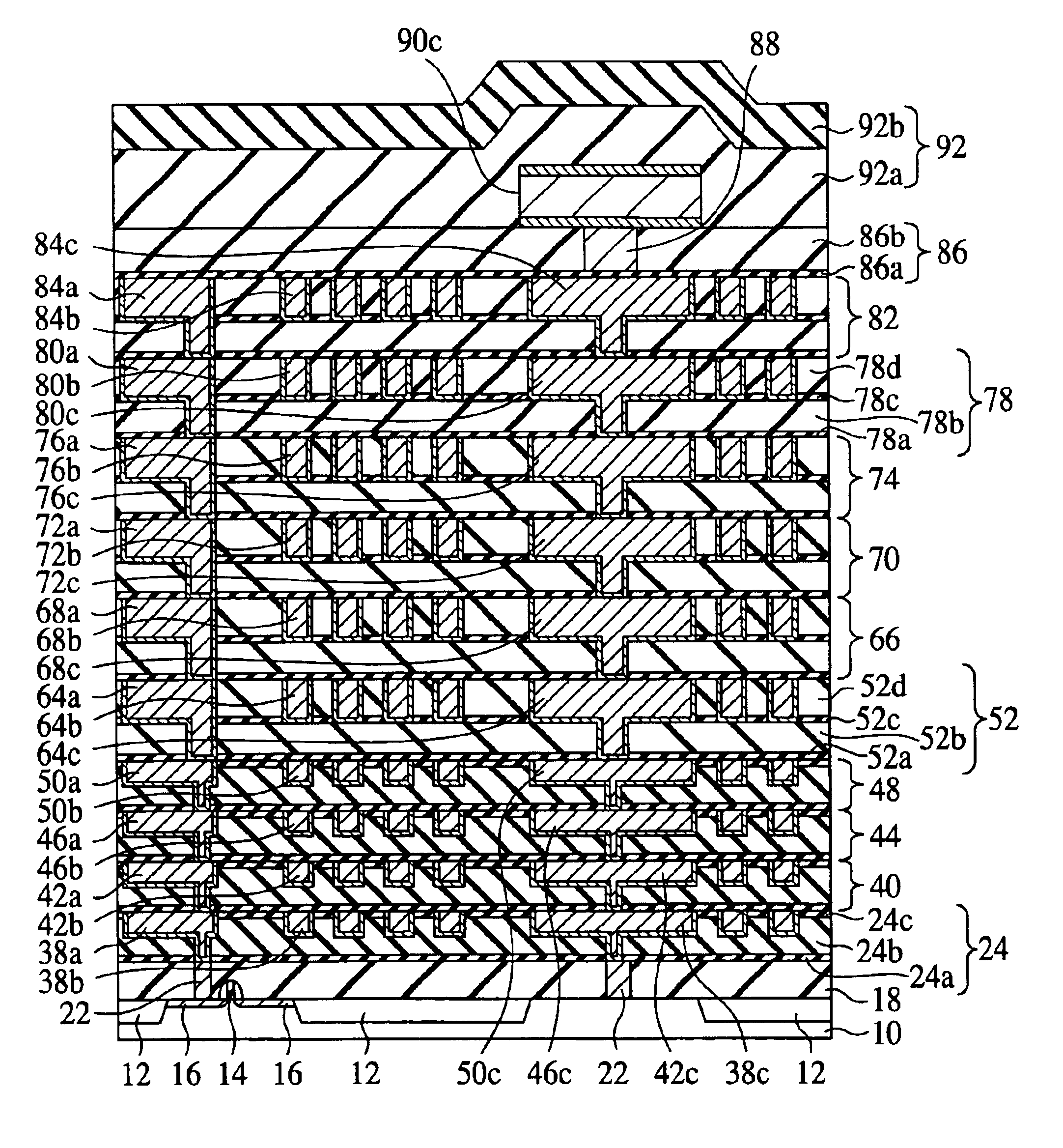
The semiconductor device according to one embodiment of the present invention will be explained with reference to FIG. 5.

FIG. 5 is a diagrammatic sectional view of the semiconductor device according to the present embodiment, which shows a structure thereof.

A device isolation film 12 is formed on a silicon substrate 10. MOS transistors each including a gate electrode 14 and source / drain diffused layers 16 are formed on the silicon substrate 10 with the device isolation film 12 formed on. An inter-layer insulating film 18 of silicon oxide, which is, e.g., undoped or doped with P (phosphorus) or B (boron), is formed on the silicon substrate 10 with the MOS transistors formed on. Contact plugs 22 of, e.g., barrier metal and W (tungsten) are buried in the inter-layer insulating film 18.

An inter-layer insulating film 24 of the layer structure of, e.g., a 30 nm-thick SiC film 24a, a 450 nm-thick SILK film 24b and a 50 nm-thick SiC film is formed on the inter-layer insula...


PUM


Abstract

The semiconductor device comprises an insulating film 114 formed mainly of a film of polyallyl ether resin; an interconnection structure 116 buried in the insulating film 114, and having a via portion buried in a groove-shaped via hole and an interconnection portion formed on the via portion and having an eave-shaped portion horizontally extended beyond the via portion; an insulating film 118 formed on the insulating film 114 with the interconnection structure 116 buried in and formed mainly of a film of organosilicate glass; and an interconnection structure 120 buried in the insulating film 118 and connected to the interconnection structure 116. Thus, the stresses to be exerted to the insulating films are decreased, the generation of cracks and peelings generated in the interfaces between the insulating films and in the insulating films due to the stresses generated at the ends of the interconnection structures can be effective prevented.

Description

CROSS-REFERENCE TO RELATED APPLICATIONSThis application is based upon and claims the benefit of priority from the prior Japanese Patent Application No. 2002-315609, filed in Oct. 30, 2002, the entire contents of which are incorporated herein by reference.BACKGROUND OF THE INVENTIONThe present invention relates to a semiconductor device comprising an inter-layer insulating film of low dielectric constant material.In semiconductor device fabrication processes, a number of elements are formed on one semiconductor wafer, and the semiconductor wafer is cut along dicing lines into discrete LSI chips. On the side walls along the dicing lines, the interfaces of many inter-layer insulating films laid in the process of forming the elements are exposed. The interfaces are often paths for water intrusion, causing problems, such as erroneous operations and breakages, etc. of semiconductor devices, which impair their reliability. Stresses in the dicing, and stresses, etc. due to thermal expansion...

Claims


Application Information

Patent Timeline
IPC IPC(8): H01L23/52H01L23/58H01L23/532H01L21/02H01L21/3105H01L21/312H01L23/522H01L21/768
CPCH01L23/5329H01L23/585H01L21/31053H01L2924/3011H01L2924/0002H01L2924/00
Inventor HOSODA, TSUTOMUYAMANOUE, AKIRA
Owner TRINITY SEMICON RES
Features
  • Generate Ideas
  • Intellectual Property
  • Life Sciences
  • Materials
  • Tech Scout
  • Unparalleled Data Quality
  • Higher Quality Content
  • 60% Fewer Hallucinations
Learn More