Multi-detector microscopic inspection system

Inactive Publication Date: 2005-03-01
KLA TENCOR CORP
View PDF16 Cites 10 Cited by
  • Summary
  • Abstract
  • Description
  • Claims
  • Application Information

AI Technical Summary

Benefits of technology

The present invention pertains to a microscope inspection system capable of inspecting specimens at high throughput rates. The inspection system achieves the higher throughput rates by utilizing more than one detector array and a large field of view to scan the surface of the semiconductor wafers. The microscope inspection system also has high magnification capabilities, a high numerical aperture, and a large field of view. By using more than one detector array, more surface area of a wafer can be inspected during each scanning swath over the semiconductor wafers thereby minimizing the swathing overhead time and making the system more efficient. The microscope inspection system is configured to have a larger field of view so that the multiple detector arrays can be properly utilized. Additionally, special arrangements of reflective and / or refractive surfaces are used in order to fit the detector arrays within the physical constraints of the inspection system.

Problems solved by technology

Semiconductor manufacturing involves highly complex techniques for integrating circuits into semiconductor materials.
Due to the large number of processing steps and the decreasing size of semiconductor devices, the semiconductor manufacturing process is prone to processing defects that decrease device yields.
Unfortunately, scanning wafers line-by-line is time consuming, especially when the time required for changing the relative directions of the detector arrays over the wafer is taken into account.
Therefore, microscopic inspection of wafers reduces the throughput of semiconductor manufacturing.
Unfortunately, larger detector arrays with no defective pixels are very difficult to fabricate because yields are small with physically large devices.
However, it is difficult to obtain much improvement from the current state-of-the-art using this strategy because the detectors create a greater amount of noise at higher speeds, thereby diminishing the signal-to-noise ratio.
This would also not help the scanning overhead time.

Method used


Image

  • Multi-detector microscopic inspection system
  • Multi-detector microscopic inspection system
  • Multi-detector microscopic inspection system

Examples


Embodiment Construction

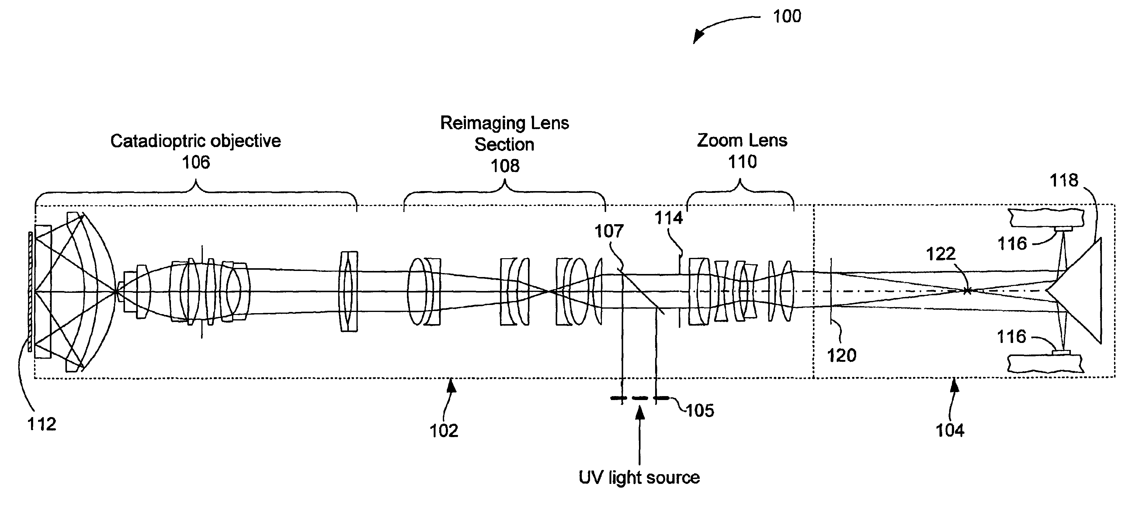
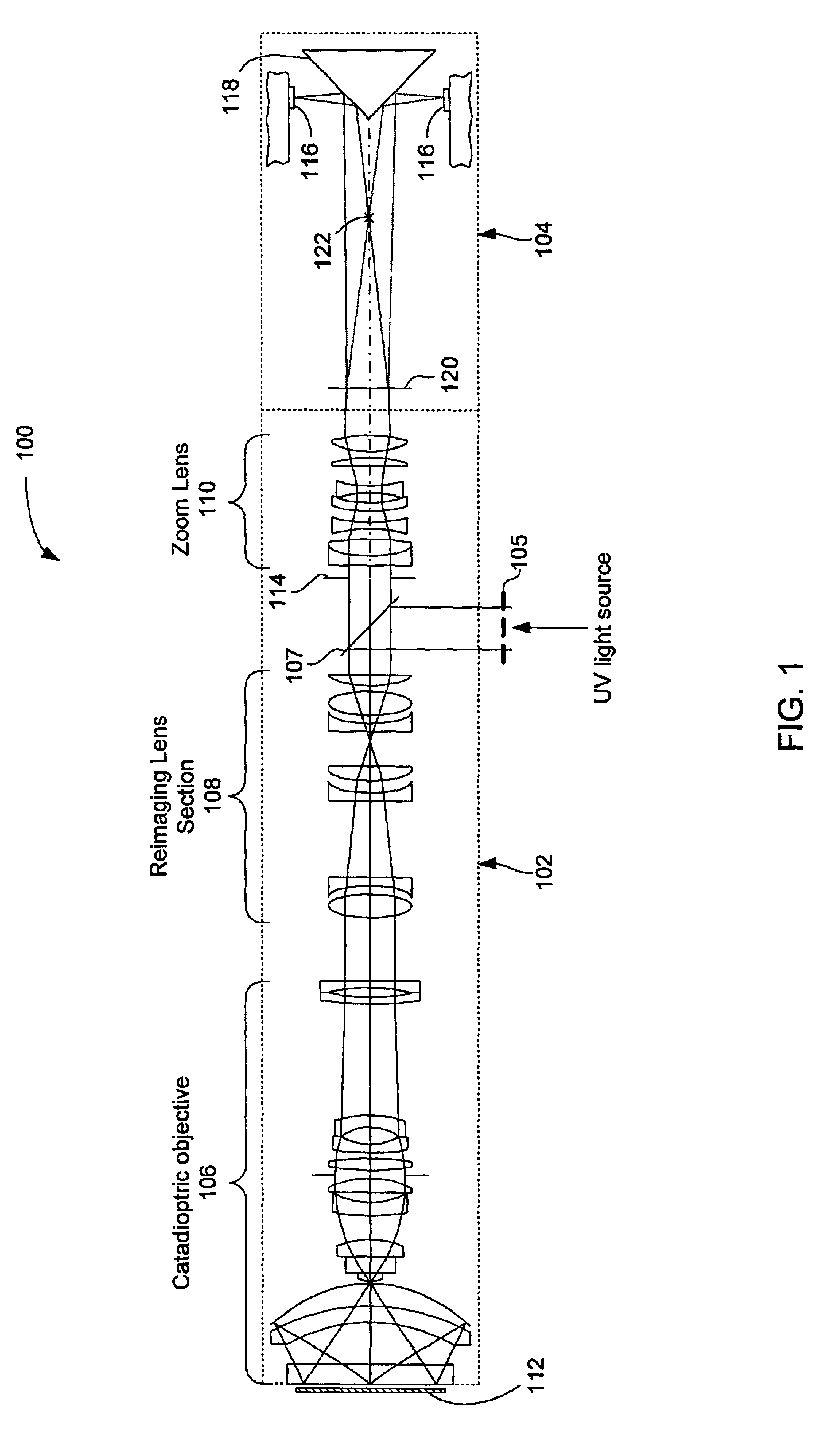
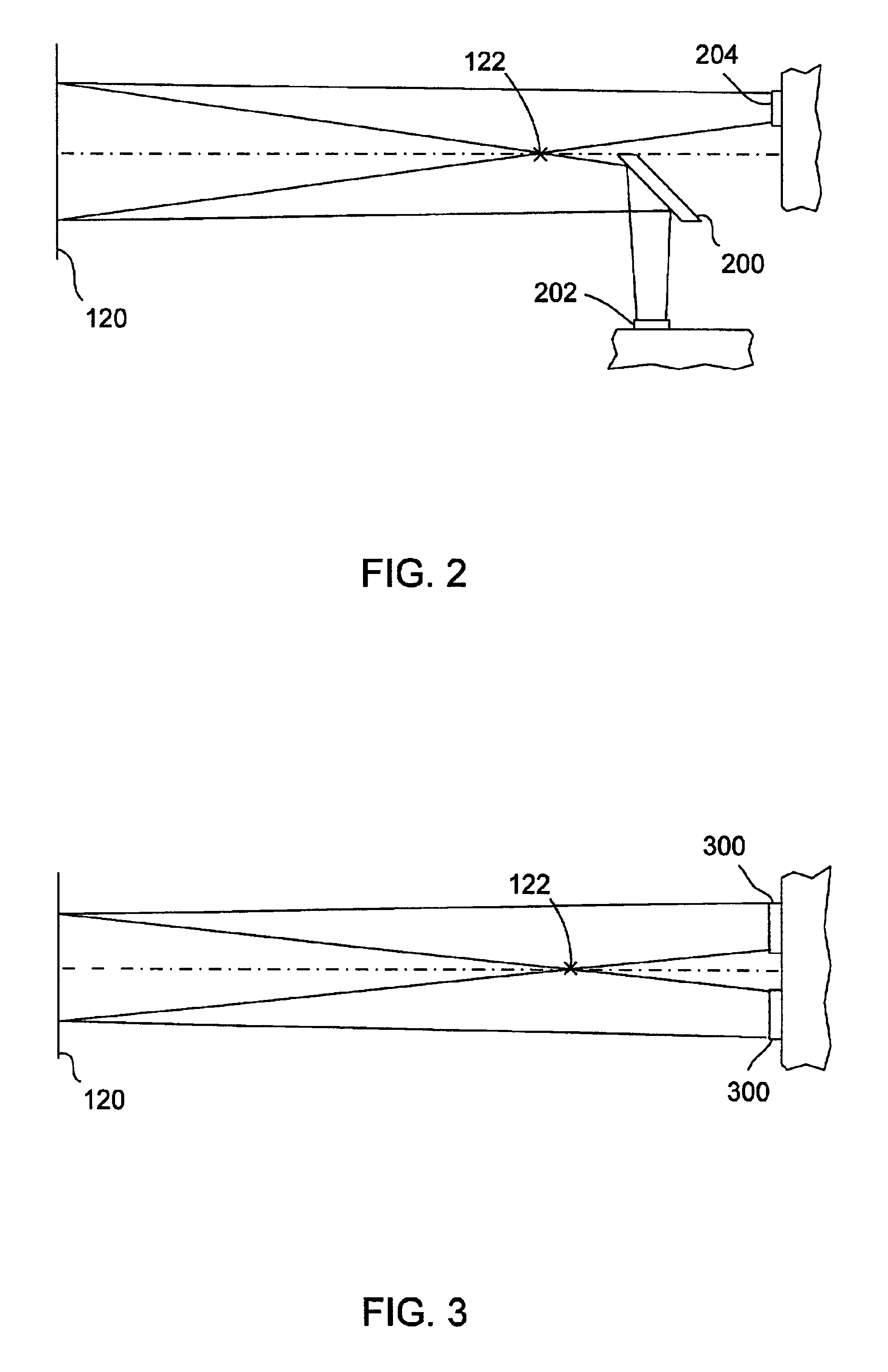
The present invention will now be described with reference to a few preferred embodiments thereof as illustrated in the accompanying drawings. In the following description, numerous specific details are set forth in order to provide a thorough understanding of the present invention. It will be apparent, however, to one skilled-in-the-art, that the present invention may be practiced without some or all of these specific details. In other instances, well-known operations have not been described in detail so not to unnecessarily obscure the present invention.

To begin with, an overview of the present invention will now be provided. The present invention pertains to a semiconductor inspection system capable of operating at high throughput rates. Generally, the inspection system achieves the higher throughput rates by utilizing more than one detector array and a large field of view to scan the surface of the semiconductor wafers. By using more than one detector array, more surface area of...


PUM


Abstract

Techniques for utilizing a microscope inspection system capable of inspecting specimens at high throughput rates are described. The inspection system achieves the higher throughput rates by utilizing more than one detector array and a large field of view to scan the surface of the semiconductor wafers. The microscope inspection system also has high magnification capabilities, a high numerical aperture, and a large field of view. By using more than one detector array, more surface area of a wafer can be inspected during each scanning swath across the semiconductor wafers. The microscope inspection system is configured to have a larger field of view so that the multiple detector arrays can be properly utilized. Additionally, special arrangements of reflective and / or refractive surfaces are used in order to fit the detector arrays within the physical constraints of the inspection system.

Description

FIELD OF THE INVENTIONThe present invention relates generally to microscopic inspection systems, and more specifically to microscopic inspection systems that utilize multiple detector arrays.BACKGROUND OF THE INVENTIONSemiconductor manufacturing involves highly complex techniques for integrating circuits into semiconductor materials. Due to the large number of processing steps and the decreasing size of semiconductor devices, the semiconductor manufacturing process is prone to processing defects that decrease device yields. Inspection procedures used to detect and eliminate these processing defects from the processing steps are therefore critical for maintaining high yielding production processes. Since the inspection procedures are an integral and significant part of the manufacturing process, the semiconductor industry constantly seeks more accurate and efficient inspection techniques.Currently, typical microscopic inspection systems utilize a single detector array to inspect semi...

Claims


Application Information

Patent Timeline
IPC IPC(8): G02B21/00G02B21/02G02B17/08G01N21/956G01Q10/00G01Q30/20G02B21/06G02B21/04G02B21/18
CPCG02B17/0808G02B17/0856G02B17/086G02B17/0892G02B21/367G02B21/025G02B21/04G02B21/18G02B21/0016
Inventor LANGE, STEVEN R.
Owner KLA TENCOR CORP
Why Eureka
Try Eureka