Methodology of generating antenna effect models for library/IP in VLSI physical design

a technology of physical design and antenna effect, applied in the field of automatic design methodology, can solve the problems of large voltage potential in the film, film charging, non-uniformity in the plasma, etc., and achieve the effect of effectiv

Inactive Publication Date: 2005-03-01
TAIWAN SEMICON MFG CO LTD
View PDF9 Cites 42 Cited by
  • Summary
  • Abstract
  • Description
  • Claims
  • Application Information

AI Technical Summary

Benefits of technology

A principal object of the present invention is to provide an effectiv...

Problems solved by technology

A well known problem with plasma etching, however, is film charging.
This charging is thought to be caused by non-uniformity in the plasma.
The accumulation of charge can cause a large voltage potential to develop in the film.
It is found that the plasma-induced charging can cause gate oxide 22 failures.
The presence of diffusion regions coupled to the metal lines has a large effect on the plasma charging problem.
However, the calculation that can be performed by the router is severely limited because the routing program has very limited information on the contents of the blocks that are being routed.
Further, no information is available to the router regarding which metal level, or levels, are coupled to these gate and source/drain areas.
However, the routing program has no visibility regarding the antenna effect information...

Method used


Image

  • Methodology of generating antenna effect models for library/IP in VLSI physical design
  • Methodology of generating antenna effect models for library/IP in VLSI physical design
  • Methodology of generating antenna effect models for library/IP in VLSI physical design

Examples


Embodiment Construction

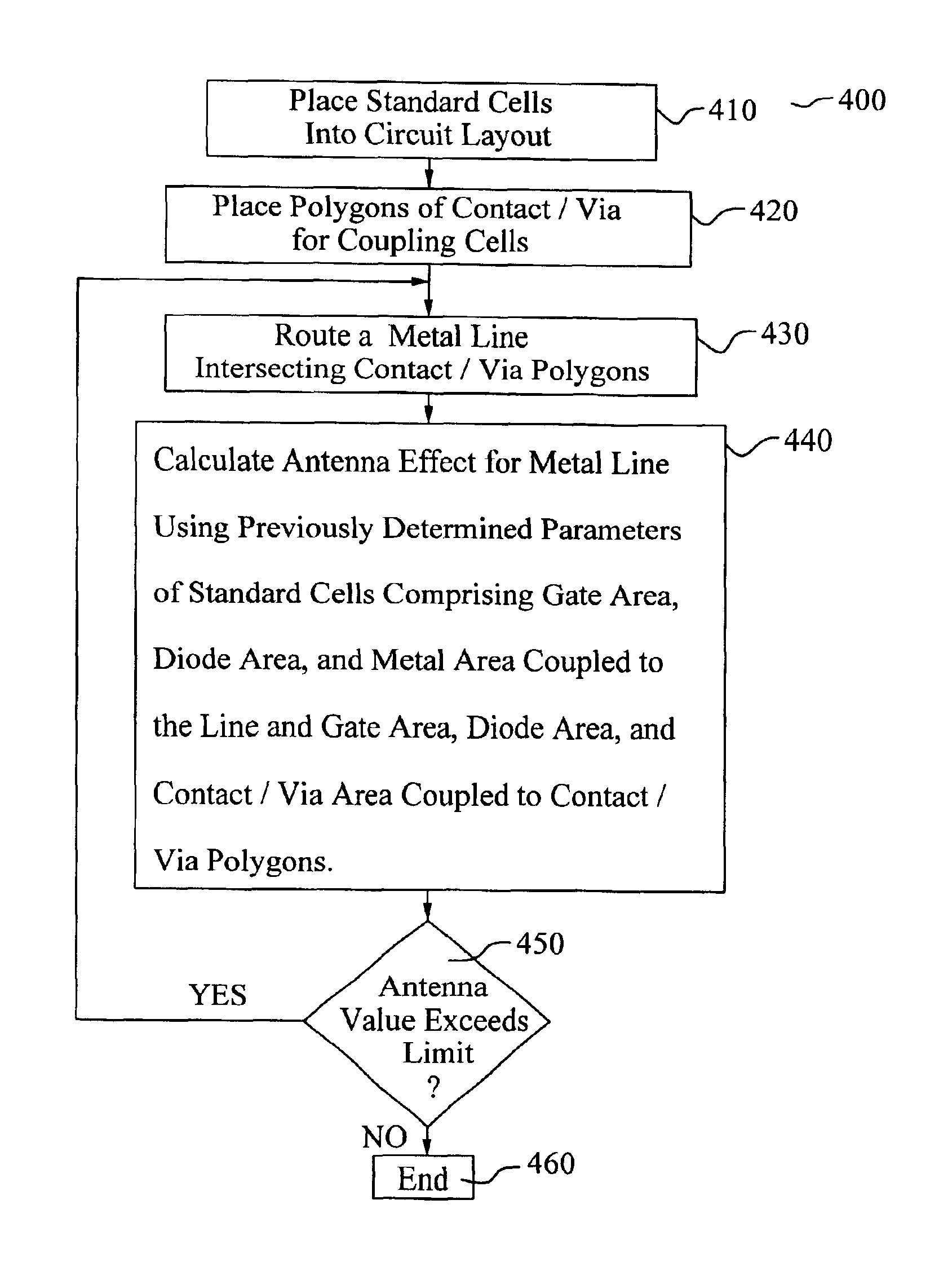
The preferred embodiments of the present invention disclose a method to extract antenna effect parameters from a standard cell or block of an integrated circuit device prior to placement and routing. The extraction method systematically analyzes the cell layout to generate parameters corresponding to each pin connection of the cell. These parameters are then available to a placement and routing program to facilitate more accurate calculation of antenna effect ratios and limits for each routed signal line. A method to use these parameters in the routing of signal lines is also disclosed. It should be clear to those experienced in the art that the present invention can be applied and extended without deviating from the scope of the present invention.

Referring now to FIG. 6, the preferred embodiment of the present invention is illustrated. Several important features of the present invention are shown and discussed below. A method 300 to determine parameters from the layout of a standar...


PUM


Abstract

A new method to route a metal line in the layout of an integrated circuit device is achieved. The method comprises providing a layout for an integrated circuit device comprising an array of placed standard cells. Contact/via layer polygons are placed for coupling the standard cells. A line is routed in a metal layer. An antenna effect value is calculated for the line using parameters previously determined from the layout of each the standard cell. The parameters comprise gate area, diode area, metal area, and contact/via area coupled to the line. The gate area, the diode area, the metal area, and the contact/via area are segregated by metal level. The steps of routing and calculating are repeated if the antenna effect value exceeds a specified value. A method to extract parameters is disclosed.

Description

BACKGROUND OF THE INVENTION(1) Field of the InventionThe invention relates to an automated design methodology and, more particularly, to a method to generate antenna effect models for standard library components for use by automatic placement and routing software.(2) Description of the Prior ArtIntegrated circuits are typically fabricated using a plurality of layers comprising different materials. These layers are formed or deposited using a variety of different processes. Frequently, these deposited layers must be further patterned to form final designs. This patterning is performed using etching processes. A particular etching process of importance in the present invention is plasma etching.Plasma etching processes comprise a gas ion plasma that is used to etch an exposed layer on an integrated circuit. These plasma etching processes may exhibit high selectivity as well as fine direction control (anisotropy). A well known problem with plasma etching, however, is film charging. In ...

Claims


Application Information

Patent Timeline
IPC IPC(8): G06F9/45G06F17/50
CPCG06F17/5081G06F17/5036G06F30/398G06F30/367
Inventor WANG, CHUNG-HSINGWANG, DAISYCHENG, CHIA LINGLU, LEE CHUNGHOU, CLIFF
Owner TAIWAN SEMICON MFG CO LTD
Why Eureka
Try Eureka