Method and apparatus for testing semiconductor devices

a technology for semiconductor devices and test cycles, applied in the direction of instruments, coding, recording signal processing, etc., can solve the problems of inability to guarantee repeatability and hence reliability of measured values, low reliability of test using such measured values, and inability to guarantee repeatability and reliability

Inactive Publication Date: 2005-03-08
ADVANTEST CORP
View PDF15 Cites 15 Cited by
  • Summary
  • Abstract
  • Description
  • Claims
  • Application Information

AI Technical Summary

Benefits of technology

[0013]It is therefore an object of the present invention to provide a semiconductor device test method that permits real-time testing from the beginning and hence reduction of the test time and ensures the reliability of test conclusions in the test of a semiconductor device of the type that uses the reference clock generated by the device itself to decide whether the phase of each piece of data is within the range of a predetermined phase difference.
[0025]Hence, the present invention offers a semiconductor device testing method and apparatus which enable semiconductor devices of the above-mentioned type to be tested in a short time and with high reliability by a relatively simple construction in which only the logical condition decider is provided in the stage following each logic comparator of a common semiconductor device tester.

Problems solved by technology

Further, since the timing of generation of the reference clock DQS contains random jitter J as depicted in FIG. 14, pre-measuring the generation timing over all the test cycles does not guarantee repeatability and hence reliability of the measured values.
Accordingly, the test using such measured values is inevitably low in accuracy and consequently in reliability.

Method used


Image

  • Method and apparatus for testing semiconductor devices
  • Method and apparatus for testing semiconductor devices
  • Method and apparatus for testing semiconductor devices

Examples


Embodiment Construction

lass="d_n">[0040]FIG. 10A is a timing chart for explaining how to test the timing of the trailing edge of data with Tb<Tdr;

[0041]FIG. 10B is a table showing the results of logical comparison by the FIG. 10A test scheme in time sequence;

[0042]FIG. 11A is a truth table for explaining the operation of a logical condition decider based on the results of comparison with the leading edge of data;

[0043]FIG. 11B is a truth table for explaining the operation of a logical condition decider based on the results of comparison with the trailing edge of data;

[0044]FIG. 12 is a block diagram for explaining an example of a concrete configuration of the logical condition decider that constitutes the principal part of the present invention;

[0045]FIG. 13 is a timing chart for explaining the problem to be solved by the present invention; and

[0046]FIG. 14 is a timing chart for explaining jitter of output data of the semiconductor device under test.

DETAILED DESCRIPTION OF THE PREFERRED EMBODIMENTS
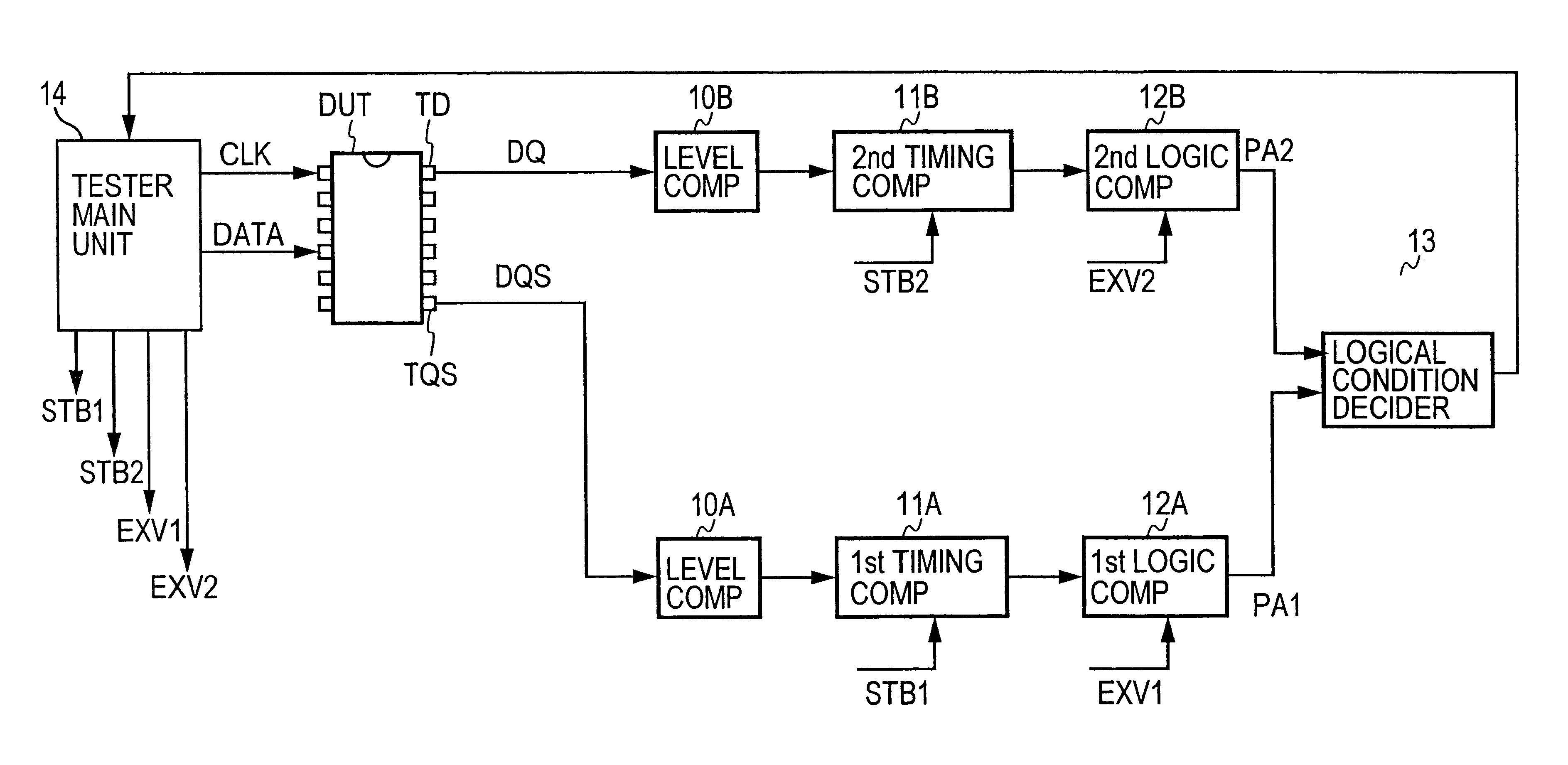
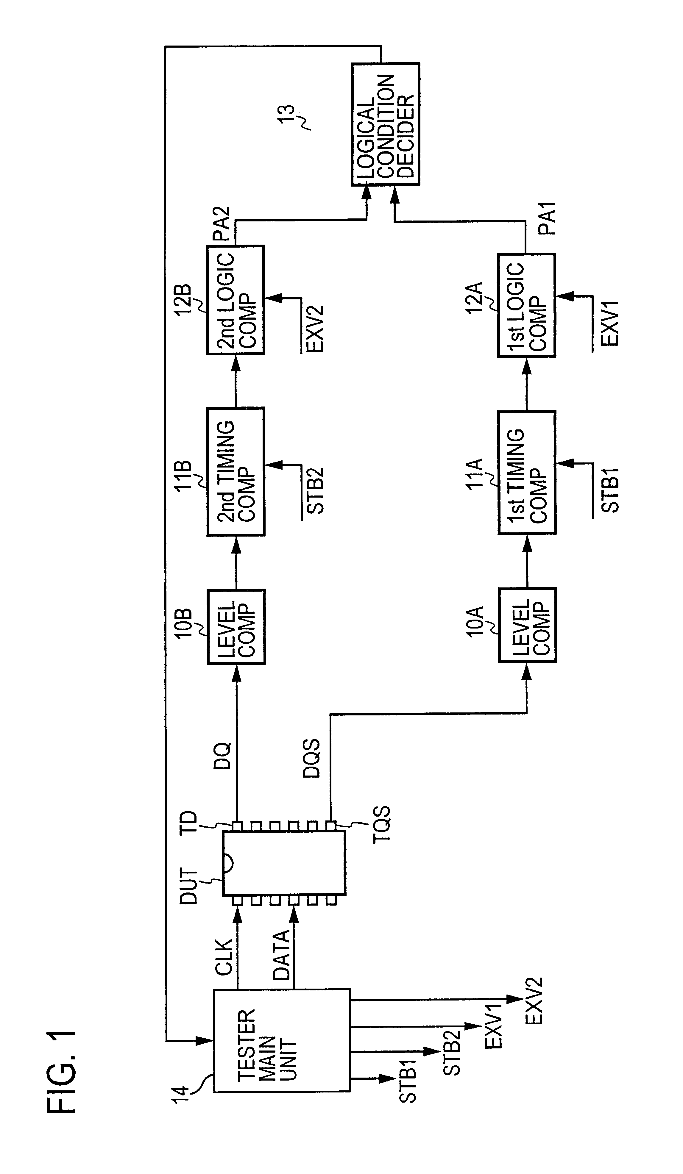
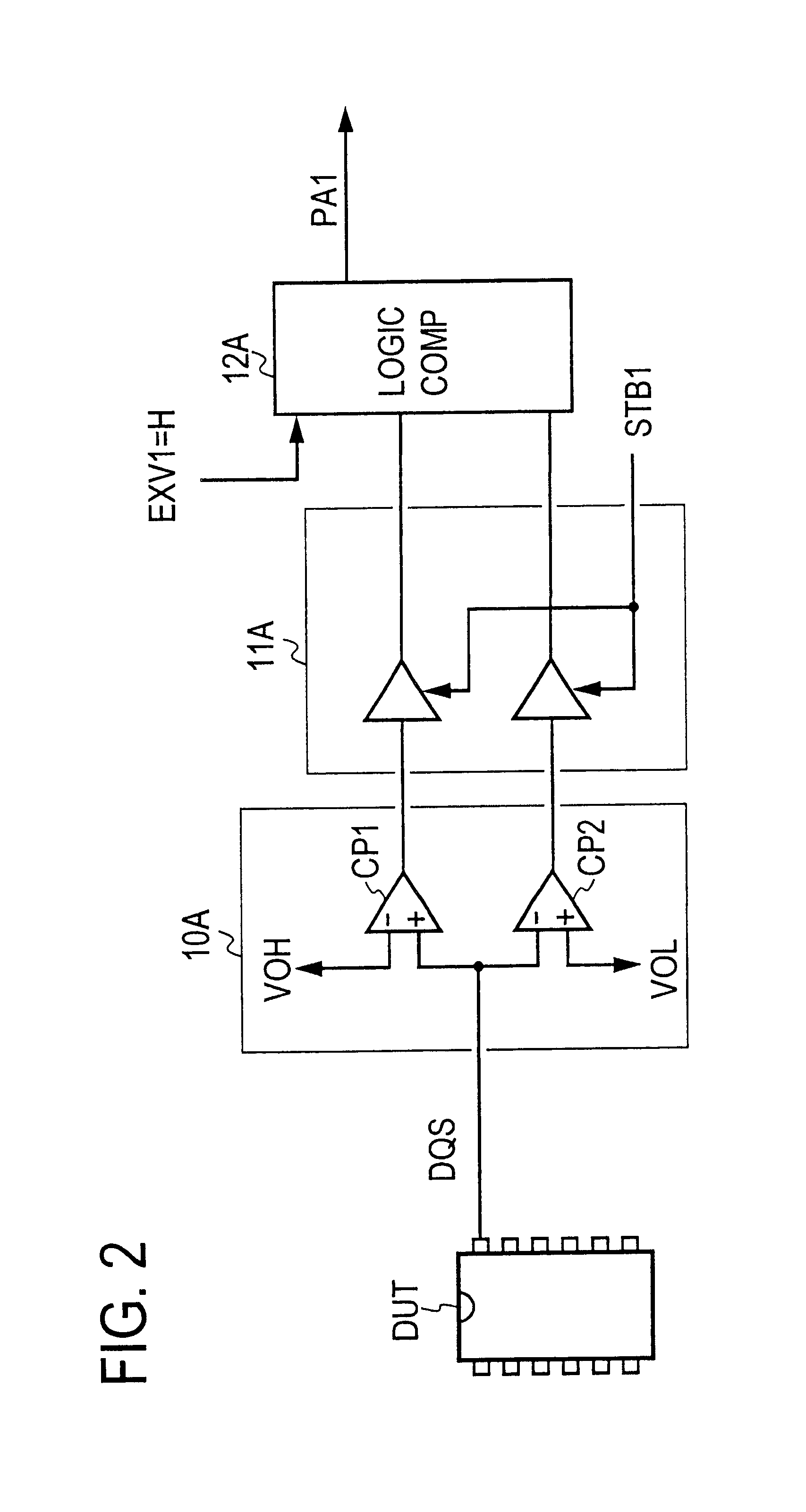
[0047]F...


PUM

PropertyMeasurementUnit
time widthaaaaaaaaaa
delay timeaaaaaaaaaa
timeaaaaaaaaaa

Abstract

In a semiconductor device which outputs read-out data and a reference clock synchronized therewith for use in passing the data to other device, the generating timing of the reference clock and the generating timing of the data are compared by timing comparators 11A and 11B with first and second strobe pulses, and the logical values of the timing comparison result are compared by logic comparators 12A and 12B with first and second expected values. A logical condition decider 13 decides whether the combination of the logical comparison results satisfies a predetermined condition. When the predetermined condition is met, the decider 13 decides that the phase difference between the reference clock and the data is larger than a predetermined value, or that the duration of the data is longer than a predetermined time.

Description

BACKGROUND OF THE INVENTION[0002]The present invention relates to a method and apparatus for testing semiconductor devices which output a reference clock and data synchronized therewith.[0003]Among a wide variety of semiconductor devices is a memory of the type that takes in data fed to a terminal together with an input clock and outputs a reference clock and data synchronized therewith. For example, a DDSRDRAM (Double Data Rate Synchronous Dynamic Random Access Memory) takes in address data provided along with an input clock, then generates a reference clock synchronized with the input clock by a DLL (Delayed Locked Loop), and outputs data read out of specified addresses in synchronization with and together with the reference clock, thereby allowing ease in passing data to other devices through utilization of the timing of the reference clock.[0004]FIG. 13 shows how this kind of memory device is read out. In FIG. 13A, reference characters DA, DB, DC, . . . denote pieces of output d...

Claims


Application Information

Patent Timeline
Patent Type & Authority Patents(United States)
IPC IPC(8): G01R31/3193G01R31/28G01R31/26G01R31/319G11C29/56
CPCG01R31/31937G01R31/3193G01R31/26G01R31/319G11C29/56
Inventor HOUSAKO, TAKAHIRO
Owner ADVANTEST CORP
Why Eureka
Try Eureka