Semiconductor device identification apparatus

a technology of device identification and identification apparatus, which is applied in the direction of electrical apparatus, instruments, and sensing record carriers, can solve the problems of inefficient scattering approach, reducing color contrast, and using a ccd-camera, and achieves high image pattern contrast and reduces erroneous reading of device identification patterns

Inactive Publication Date: 2005-03-15
POLARIS INNOVATIONS
View PDF28 Cites 5 Cited by
  • Summary
  • Abstract
  • Description
  • Claims
  • Application Information

AI Technical Summary

Benefits of technology

A semiconductor device identification apparatus can reduce erroneous reading of device identification patterns due to discolorations, while providing a high image pattern contrast for a large range of dot profiles. In particular, a semiconductor device identification apparatus for reading an identification pattern from the surface of a semiconductor device, in which identification pattern includes a matrix of holes or elevations formed in s

Problems solved by technology

The approach using a CCD-camera has several disadvantages under productive circumstances.
Such a ring running through a laser dot or hole can result in a non-detection of the corresponding matrix element, thereby issuing an error signal if the corresponding wrong wafer identification is currently not expected at the processing tool.
Moreover, dust particles due to previous processing may have deposited inside the engraved holes, thereby additionally decreasing the color contrast, which is necessary for the optical CCD-camera appr

Method used


Image

  • Semiconductor device identification apparatus
  • Semiconductor device identification apparatus
  • Semiconductor device identification apparatus

Examples


Embodiment Construction

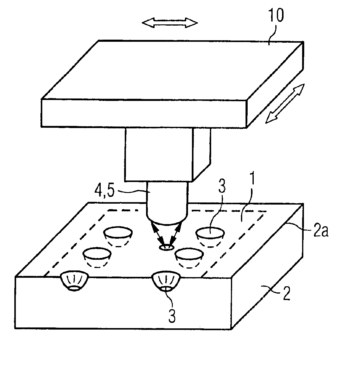
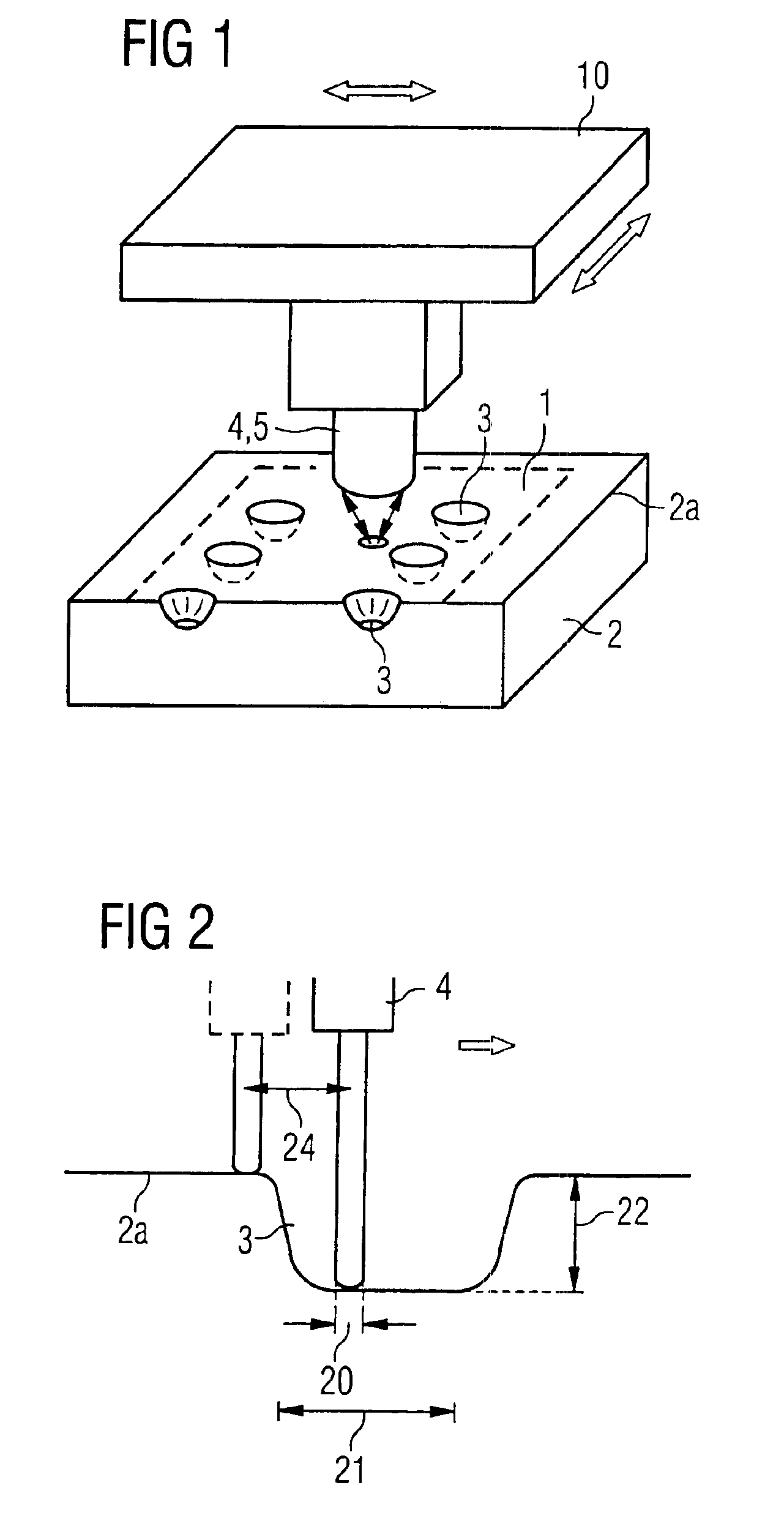
The source of radiation 4, which can be a laser, and a sensor 5 can be mounted on a stage 10, as shown in FIG. 1. The stage 10 can provide a scanning movement in both x- and y-direction at a constant height level above a semiconductor device 2 having a surface 2a, on which an identification pattern 1 is structured by an arrangement of laser-engraved holes 3. The semiconductor device 2, according to this embodiment, can be a semiconductor wafer and the surface 2a can be the wafer backside surface, and the identification pattern 1 is to be read out for performing an identification in, e.g., a sorter or another semiconductor processing tool.

A side view of the scanning procedure is shown in FIG. 2. For illustrating the distance measurement, a cut is performed through the position of a hole 3 being engraved into the surface 2a. Two scanning steps having a scanning pitch 24, e.g., the horizontal distance between two laser beams, can be visualized in FIG. 2. The source of radiation, i.e., ...


PUM


Abstract

A three-dimensional image of a semiconductor device identification pattern is obtained by measuring the distance of at least one sensor to the surface of the semiconductor device. The apparatus includes a source of radiation for deriving the distance from properties of the reflected light. A unit for determining the distance and an image processing unit are used to establish the three-dimensional picture. Positional information can be achieved in a scanning movement from motors being controlled by a control unit. By applying a threshold value, a two-dimensional image is derived and by a pattern recognition algorithm, the identification pattern can be analyzed.

Description

FIELD OF THE INVENTIONThe present invention relates to a semiconductor device identification apparatus for reading an identification pattern from the surface of a semiconductor device in a processing tool.BACKGROUNDIn semiconductor device manufacturing, in particular, semiconductor wafers, it is often necessary to track single devices or lots through their sequence of processing steps. For this reason, each device is marked with a device identification number comprising, e.g., the lot name and the device number. In case of entering a processing tool, the device identification supplied on the device surface is read out in order to check, whether the correct device is currently being processed, and perhaps information is retrieved from a database, whether specific actions are to be taken for the current device.In the case of semiconductor wafers as an example, single wafer tracking is enabled by engraving the wafer identification onto the wafer backside surface in, e.g., the form of a...

Claims


Application Information

Patent Timeline
IPC IPC(8): G01B11/06G01B11/02H01L21/00
CPCG01B11/02H01L21/67294G01B11/0608
Inventor MARX, ECKHARDPEITER, MARTIN
Owner POLARIS INNOVATIONS
Why Eureka
Try Eureka