Floating chip photonic device and method of manufacture

a photonic device and floating chip technology, applied in the direction of discharge tube/lamp details, discharge tube luminescnet screens, lighting and heating apparatus, etc., can solve the problems of inefficiency, low light intensity of these devices, and light from all exposed surfaces, so as to improve thermal conductivity and refractive index of the device

Inactive Publication Date: 2005-03-15
GENERAL ELECTRIC CO
View PDF15 Cites 71 Cited by
  • Summary
  • Abstract
  • Description
  • Claims
  • Application Information

AI Technical Summary

Benefits of technology

One advantage of the present invention resides in an optic buffer or spacer blended with thermally conductive fillers to improve thermal conductivity and the refractive index of the device.
Another advantage of the present invention resides in the ability to blend phosphor particles within the suspension media for down conversion and scattering of LED emissions.
Yet another advantage of the present invention resides in the surrounding of the LED chip by the suspension media providing a channel for the light output from all surfaces of the chip.
Still further advantages and benefits of the invention will become apparent to those of ordinary skill in the art upon reading and understanding the following detailed description of the preferred embodiments.

Problems solved by technology

Indeed, such devices emit light from all exposed surfaces when injected with an appropriate input current.
Undesirably however, the light emitted by these devices tends to be of relatively low intensity due to scattering and / or absorption.
This inefficiency has been recognized, and effort has been directed towards solving this particular problem.

Method used


Image

  • Floating chip photonic device and method of manufacture
  • Floating chip photonic device and method of manufacture
  • Floating chip photonic device and method of manufacture

Examples


Embodiment Construction

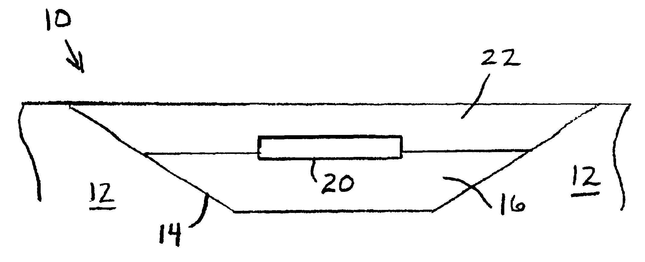
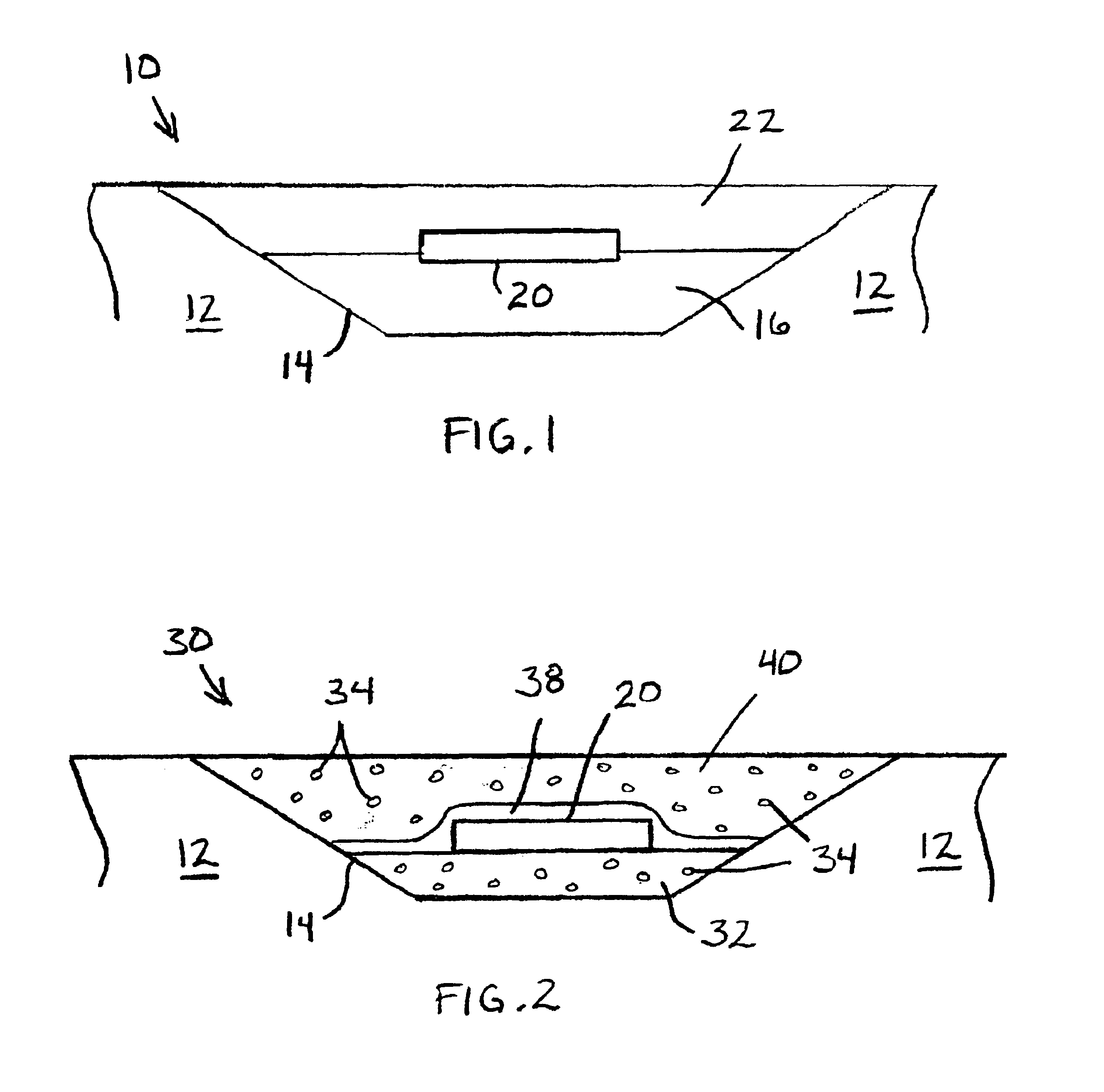
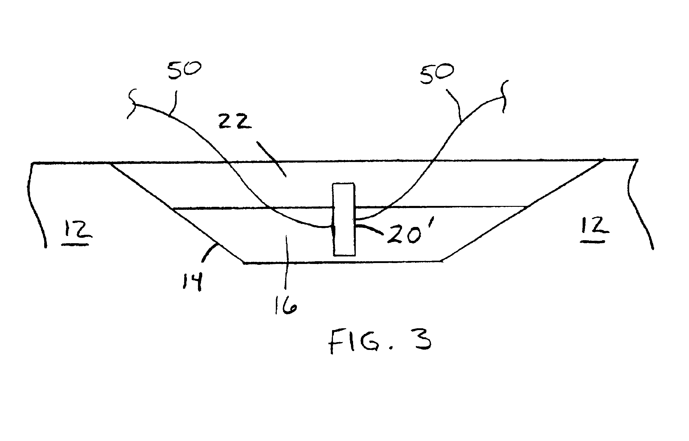
With reference to FIG. 1, a photonic device 10 such as the LED illustrated includes a metal mount 12 defining a mounting area or cup 14. A first layer of suspension media 16, such as silicone epoxy, is deposited into the cup 14. Those skilled in the art will appreciate that the silicone epoxy 16 can be pure or filled with additives to improve thermal conductivity, to adjust the refractive index, and / or to down convert the emission from an LED and scatter light. The viscosity of the silicone epoxy 16 is adjusted, for example by fillers or mild curing, to an extent that a deposited LED chip will stick to and sit upon the first layer 16 without settling appreciably. At this point, an LED chip 20 is placed upon the first layer 16. Either an upper face (with an electrode pad), or a bottom face (sapphire) of the LED chip 20 is usable in this configuration as a mounting face. Those skilled in the art will appreciate that if electrical leads were not previously applied to the LED chip 20, s...


PUM


Abstract

A solid state lamp includes a mounting area adapted to contain a light emitting diode (LED) chip and a suspension media which physically isolates the diode from the mounting area. The suspension media, while substantially optically transparent, includes suspended phosphor particles for down conversion and scattering of LED emissions. Additionally, the suspension media includes thermal conductivity additives to improve device thermal conductivity in higher power operations.

Description

BACKGROUND OF THE INVENTIONThe present invention relates to the art of solid state lamp assemblies. It finds particular application in conjunction with Light Emitting Diodes (LED's), and will be described with particular reference thereto. It is to be appreciated, however, that the present invention is also amenable to other types of light emitting semiconductor devices.Solid state lamp assemblies such as LEDs are typically made from a flat chip of material, such as III-V nitrides gallium arsenide, and / or phosphides and silicon carbide, suitably doped with material or designed so as to form a p-n junction which emits light when current is passed therethrough. Indeed, such devices emit light from all exposed surfaces when injected with an appropriate input current. Undesirably however, the light emitted by these devices tends to be of relatively low intensity due to scattering and / or absorption.This inefficiency has been recognized, and effort has been directed towards solving this p...

Claims


Application Information

Patent Timeline
Patent Type & Authority Patents(United States)
IPC IPC(8): H01J1/62H01J1/00H01L33/00H01L33/50H01L33/54
CPCH01L33/644H01L33/56H01L33/54H01L33/50
Inventor SUN, XIAO-DONGMINNEAR, WILLIAM P.
Owner GENERAL ELECTRIC CO
Why Eureka
Try Eureka