Parametric device for wavelength conversion

a wavelength conversion and parametric technology, applied in the field of parametric devices for wavelength conversion, can solve the problems of constructive and destructive interference, difficult to obtain phase matching conditions, etc., and achieve the effect of low scattering loss and high differen

Inactive Publication Date: 2005-03-15
GOOGLE LLC
View PDF17 Cites 3 Cited by
  • Summary
  • Abstract
  • Description
  • Claims
  • Application Information

AI Technical Summary

Benefits of technology

Moreover, the Applicant notes that the device of the invention having the above substantially periodic photonic crystal structure made of the alternance of four layers has the necessary flexibility to carry out a parametric process in phase matching conditions and according to the application required for the device.
Typically, the output means of the device of the invention comprises an optical filter connected to the substantially periodic structure, suitable to let the radiation generated at frequency ωg exit from the device and to suppress a possible residual pump radiation at frequency ωp and a possible residual signal radiation at frequency ωs.

Problems solved by technology

However, the phase matching condition is difficult to obtain in materials having non-linearity of the ω2 or ω3 type since such materials are typically dispersive, that is, they have a refractive index variable with the frequency ω.
The multiple reflections at the interfaces between the two layers at different refractive index generate constructive and destructive interferences between the transmitted light and the reflected light, and make the photonic crystal structure allow the propagation of electromagnetic waves in some intervals of frequencies (or wavelengths) and forbid it in other intervals.
The Applicant has thus faced the technical problem of providing a device comprising a photonic crystal structure capable of performing a difference frequency generation parametric process in phase matching conditions.

Method used


Image

  • Parametric device for wavelength conversion
  • Parametric device for wavelength conversion
  • Parametric device for wavelength conversion

Examples


Embodiment Construction

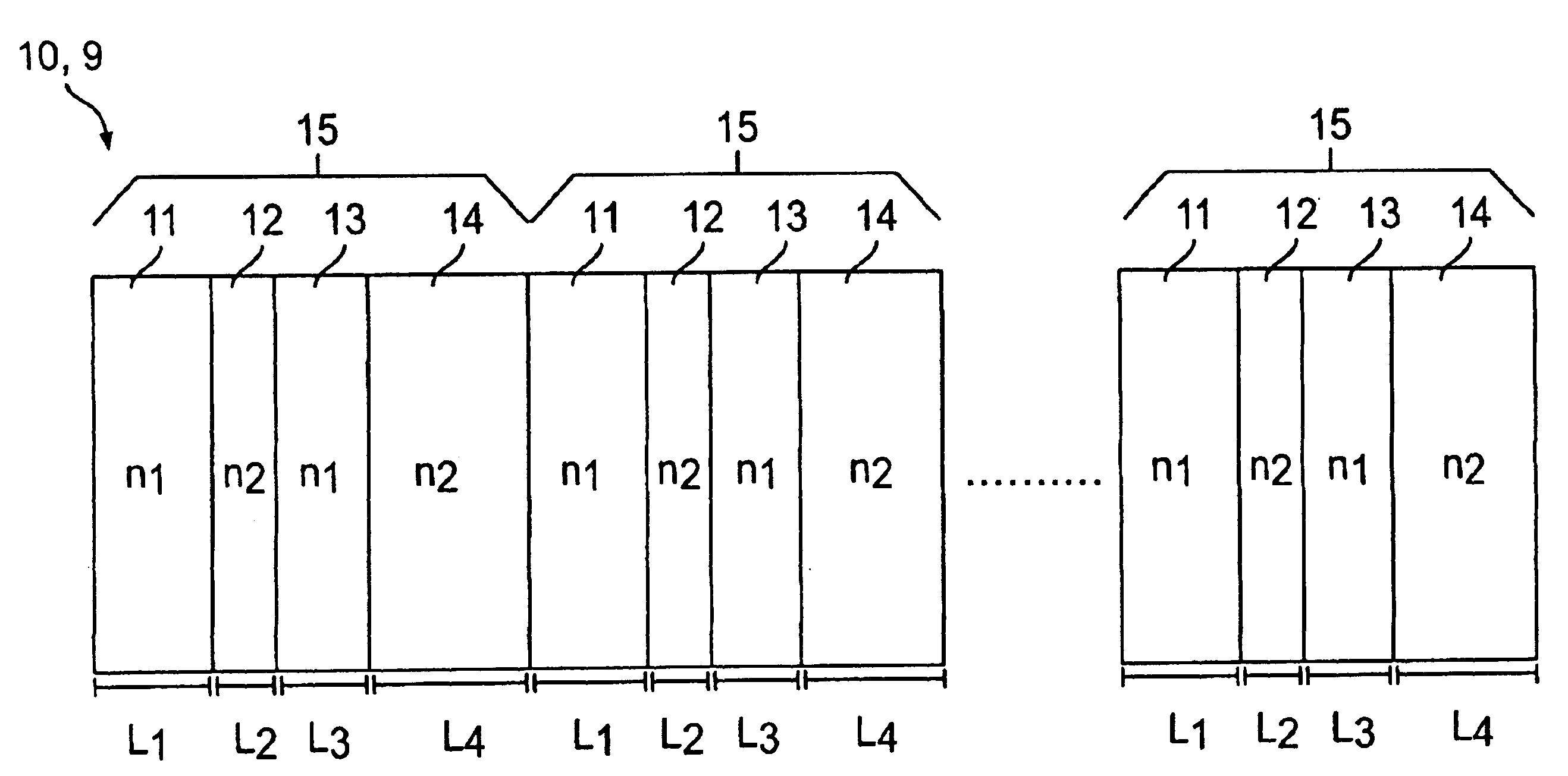
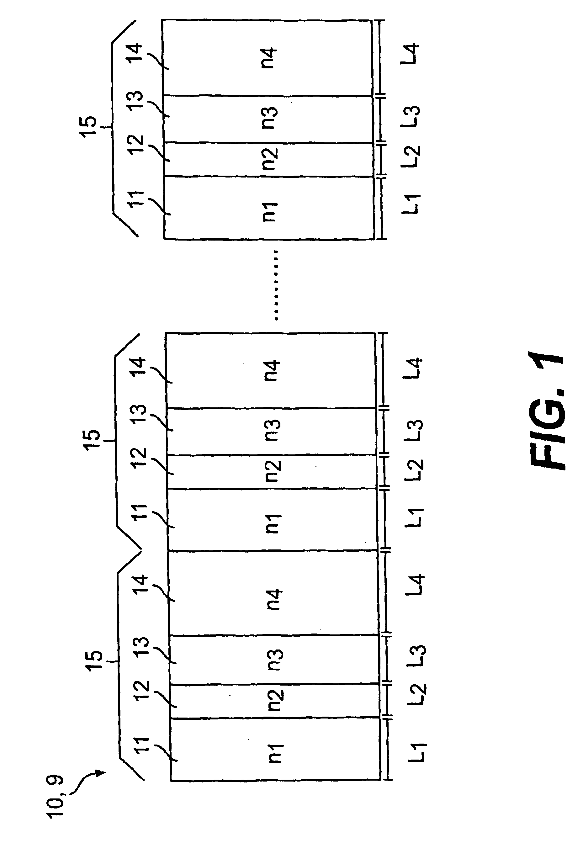
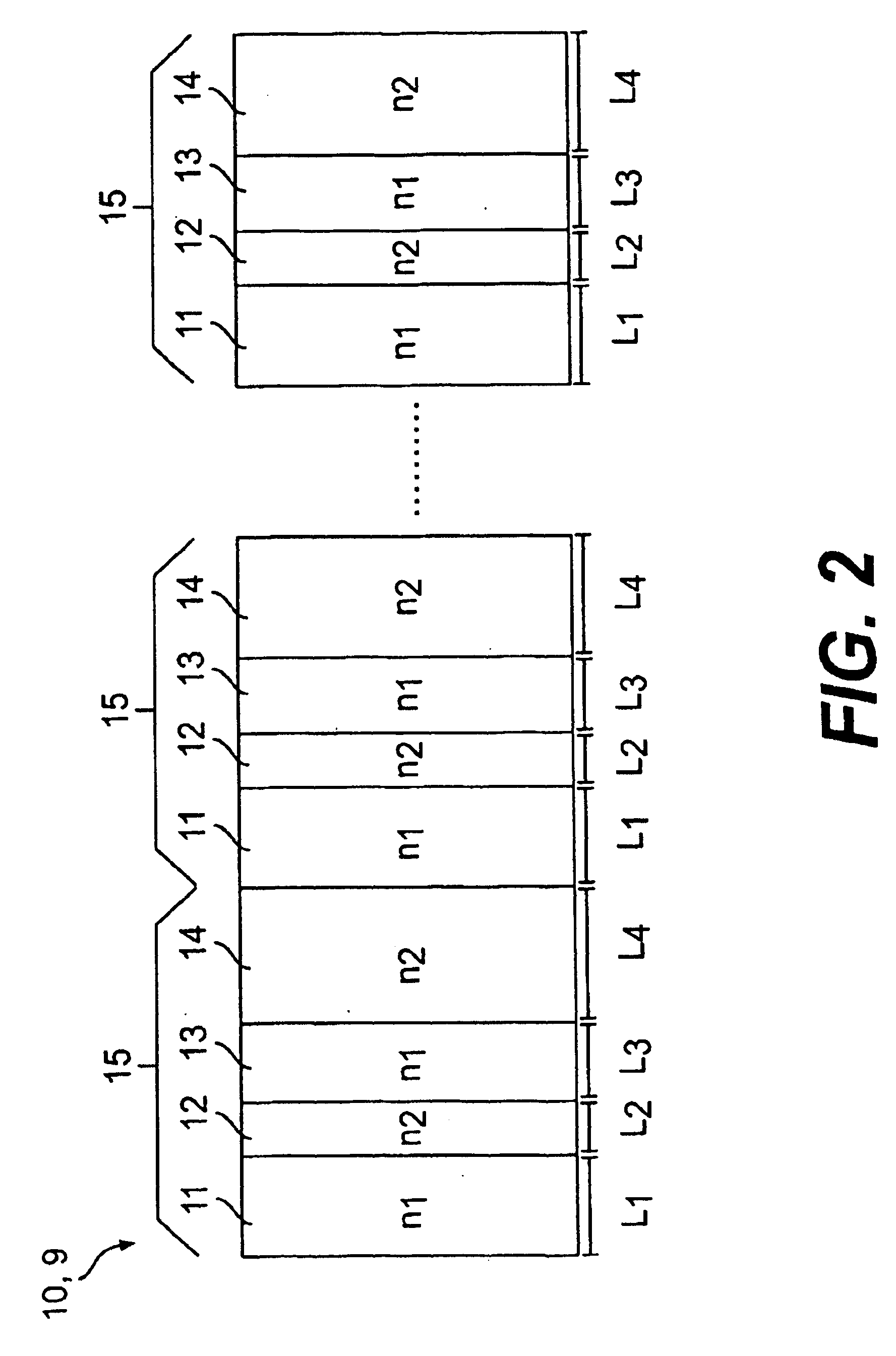
FIG. 1 shows a schematic view of a one-dimensional photonic crystal structure 9 of a device 10 according to the invention, comprising N substantially equal unitary cells 15.

Each unitary cell 15 comprises, in turn, four layers 11-14 having refractive index n1, n2, n3, n4 and lengths L1, L2, L3, L4 that periodically alternate along the photonic crystal periodic structure 9.

At least one of the four layers 11-14 consists of a material having a non-linearity of the χ2 or χ3 type so as to be able to carry out a parametric process.

The values of the refractive indices n1-n4 and of lengths L1-L4 are selected, as it will be better described in detail hereinafter, so as to perform the parametric process in phase matching conditions and according to the desired application for the device 10.

The values of the refractive indices n1-n4 and of lengths L1-L4, in fact, determine the amplitude and the position in frequency (or wavelength) of the transmission bands and of the band gaps of the transmiss...


PUM

PropertyMeasurementUnit
refractive indices n1aaaaaaaaaa
wavelengthaaaaaaaaaa

Abstract

Device for performing a parametric process, comprising a substantially periodic photonic crystal structure comprising a plurality of unitary cells each comprisinga first layer having a first refractive index n1 and a first length L1, a second layer having a second refractive index n2, with n1 different from n2, and a second length L2, a third layer having a third refractive index n3, with n3 different from n2, and a third length L3 anda fourth layer having a fourth refractive index n4, with n4 different from n1 and from n3, and a fourth length L4,  whereinat least one among the first, the second, the third and the fourth layers has a non-linearity of the χ2 or χ3 type;at least one of the following conditions is met: a) n1 is different from n3;  b) n2 is different from n4;  c) L1 is different from L3;  d) L2 is different from L4; andn1, n2, n3, n4, L1, L2, L3, L4 have such values as to perform the parametric process in phase matching conditions.

Description

BACKGROUND OF THE INVENTION1. Field of the InventionThe present invention relates to a device for performing a parametric process comprising a photonic crystal periodic structure.The present invention relates, moreover, to an optical communication line and an optical communication system comprising such device.2. Description of the Related ArtA parametric process is a typical process of materials having a non-linearity of the χ2 or χ3 type according to which electromagnetic radiations at predetermined frequencies that propagate in such materials interact with each other for generating electromagnetic radiations at different frequencies from those that have generated them (Amnon Yariv, “Optical Electronics”, Third Edition, 1985, HOLT, REINEHART and WINSTON, pages 227-236).For example, a parametric process is a process according to which a pump radiation at frequency ωp that propagates in a non-linear material, interacting with a signal radiation at frequency ωs, generates a radiation...

Claims


Application Information

Patent Timeline
Patent Type & Authority Patents(United States)
IPC IPC(8): G02F1/39G02B6/122G02F1/35
CPCB82Y20/00G02B6/1225G02F1/3544G02F1/395G02F2202/32G02F1/3534
Inventor ROMAGNOLI, MARCOSOCCI, LUCIANOCORSINI, RAFFAELEMIDRIO, MICHELE
Owner GOOGLE LLC
Why Eureka
Try Eureka