Semiconductor laser device, method of fabricating the same, and optical pickup employing the same

a semiconductor laser and laser device technology, applied in the direction of semiconductor lasers, optical beam sources, semiconductor laser structural details, etc., can solve the problems of high cost, complicated fabrication methods, and increased packaging thickness, and achieve the effect of satisfying the connection of wires

Inactive Publication Date: 2005-03-15
SHARP KK
View PDF6 Cites 6 Cited by
  • Summary
  • Abstract
  • Description
  • Claims
  • Application Information

AI Technical Summary

Benefits of technology

According to the present invention, as described above, wires are connected by application of heat thereto with a heater kept in contact with the parts of the leads exposed through openings formed in the insulatin

Problems solved by technology

This requires a complicated fabrication method and high costs.
In a package of a lead frame type, increasing the number of leads results in increasing the thickness of the package and thus the thickness of the optical pickup that employs it.
Moreover, increasing the size of the package results in increasing the costs of the metal and resin materials thereof and thus the overall costs thereof In particular, the hologram element 411 is expensive, and therefore it is desirable to make it as small as possible in order to minimize costs.
However, in the structure shown in FIGS. 17A, 17B, and 18, since the hologram element 411 serves also as a cap, increasing the size of the package results in making its peripheral portions accordingly and unduly large.
This leads to higher costs.
However, when the lead frame in the form of continuous hoops is wound up or set on equipment, if the island plates are held by only one lead pin each, those leads may bend, causing the island plates to be displaced relative to the frame portions.
Thus, while one of these three lead pins is effecti

Method used


Image

  • Semiconductor laser device, method of fabricating the same, and optical pickup employing the same
  • Semiconductor laser device, method of fabricating the same, and optical pickup employing the same
  • Semiconductor laser device, method of fabricating the same, and optical pickup employing the same

Examples


embodiment 1

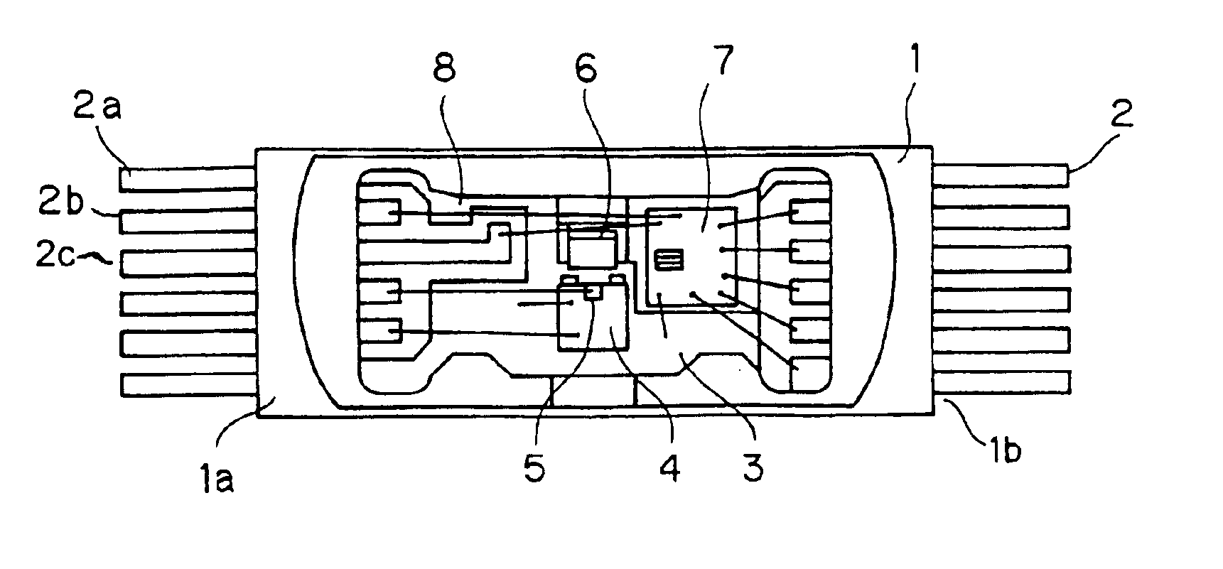
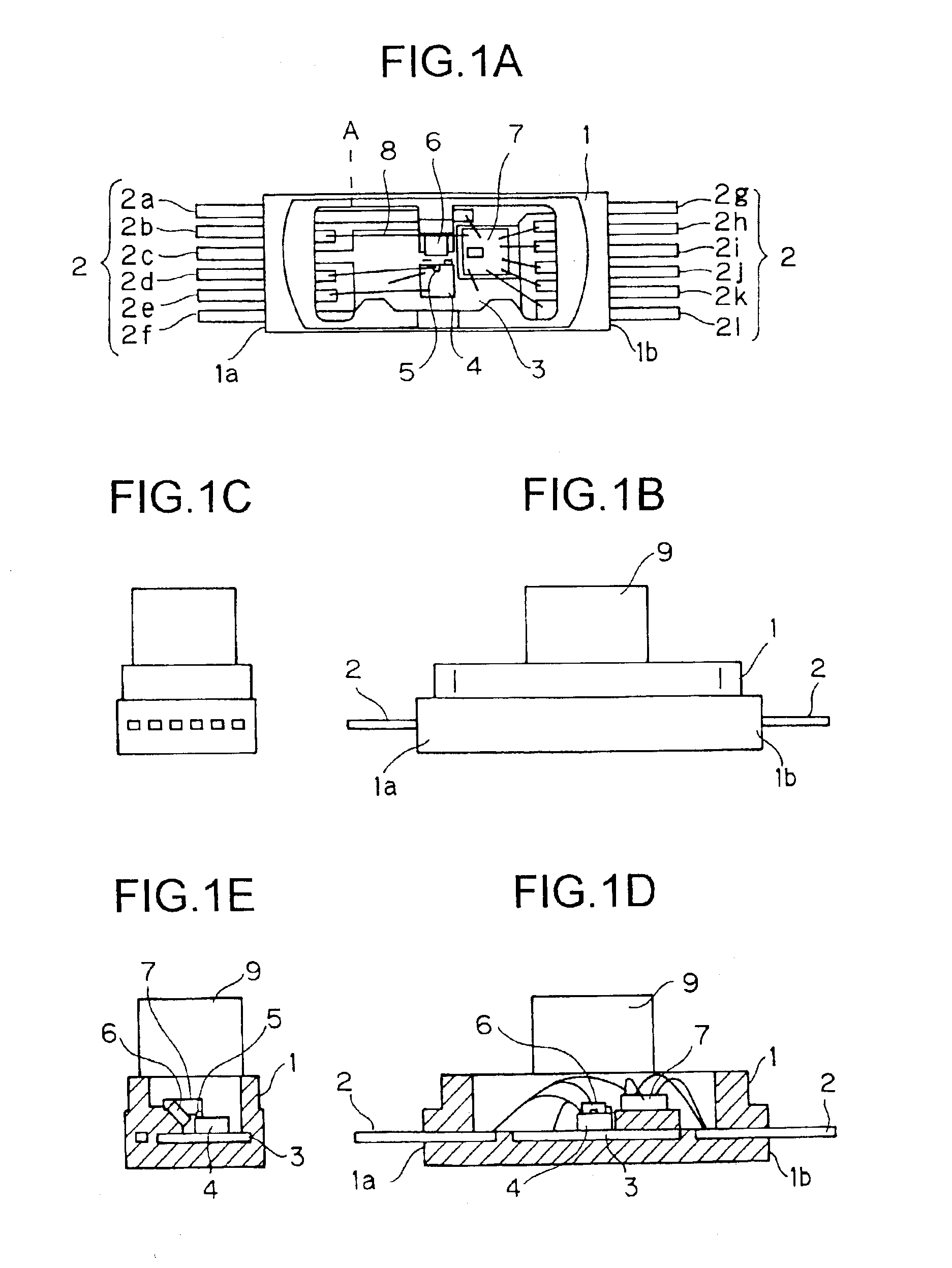
FIGS. 1A to 1E are diagrams showing an outline of the structure of the semiconductor laser device of a first embodiment (Embodiment 1) of the invention. FIG. 1A is a top view without the hologram element fitted, FIGS. 1B and 1C are side views with the hologram element fitted, and FIGS. 1D and 1E are schematic side sectional views with the hologram element fitted.

As shown in FIGS. 1A to 1E, the semiconductor laser device of this embodiment includes a plurality of leads 2 (2a to 2l) disposed through each of two sides 1a and 1b of an insulating frame member 1 so as to run from outside to inside it, a semiconductor laser element (LD) 5 and a signal-detecting light-receiving element 7 mounted inside the insulating frame member 1, and wires 8 laid inside the insulating frame member 1 so as to connect the leads 2a to 2l to the electrodes of the semiconductor laser element 5 and the light-receiving element 7. Inside the frame member, the tip of the lead 2a is extended farther inward than th...

embodiment 2

FIG. 4 is a top view showing an outline of the structure of the semiconductor laser device of a second embodiment (Embodiment 2) of the invention, without the hologram element fitted.

This embodiment differs from Embodiment 1 described above only in the leads 2a and 2c. In other respects, this embodiment is the same as Embodiment 1 described above, and therefore only the differences will be described below. In the following description, the same reference numerals as in FIGS. 1A to 1E are used irrespective of whether they appear in FIG. 4 or not.

The semiconductor laser device of this embodiment includes a plurality of leads 2 disposed through each of two sides 1a and 1b of an insulating frame member 1 so as to run from outside to inside it, a semiconductor laser element (LD) 5 and a signal-detecting light-receiving element 7 mounted inside the insulating frame member 1, and wires laid inside the insulating frame member 1 so as to connect the leads 2 to the electrodes of the LD 5 and ...

embodiment 3

FIG. 5 is a top view showing an outline of the structure of the semiconductor laser device of a third embodiment (Embodiment 3) of the invention, without the hologram element fitted.

This embodiment differs from Embodiment 1 described earlier only in the leads 2a and 2c and the relay electrode 11. In other respects, this embodiment is the same as Embodiment 1 described earlier, and therefore only the differences will be described below. In the following description, the same reference numerals as in FIGS. 1A to 1E are used irrespective of whether they appear in FIG. 5 or not.

The semiconductor laser device of this embodiment includes a semiconductor laser element (LD) 5 and a signal-detecting light-receiving element 7 mounted inside an insulating frame member 1, and, inside the insulating frame member 1, the electrodes of the LD 5 and the signal-detecting light-receiving element 7 are electrically connected to leads 2. Moreover, inside the insulating frame member 1, a relay electrode ...


PUM


Abstract

A semiconductor laser device that is suitable for mass production, that permits an improved wire layout, and that permits miniaturization includes leads disposed through each of two side faces of an insulating frame member so as to run from outside to inside the insulating frame member, an LD and a light-receiving element mounted inside the insulating frame member, and wires laid inside the insulating frame member so as to connect the leads to the electrodes of the LD and the light-receiving element. Inside the insulating frame member, the tip of one lead is extended farther inward than the edge of an element mount portion that faces the tip of another lead that is disposed through the same side face of the insulating frame member.

Description

BACKGROUND OF THE INVENTION1. Field of the InventionThe present invention relates to an optical pickup for reading information recorded on an optical recording medium, to a semiconductor laser device employed in such an optical pickup, and to a method of fabricating such a semiconductor laser device.2. Description of the Prior ArtOptical pickup devices are used in optical memory devices, such as CD-ROM drives and MD drives, to read a signal from an optical disk, and some of them adopt semiconductor laser devices of a hologram laser type. A semiconductor laser device of a hologram laser type has a semiconductor laser element, a hologram element, and a signal-detecting light-receiving element built into a single package. The light emitted from the semiconductor laser element is reflected back from a disk used as an optical recording medium, and is then diffracted by the hologram element so as to be directed to the light-receiving element disposed away from the optical axis.For example...

Claims


Application Information

Patent Timeline
IPC IPC(8): H01S5/02H01S5/00H01S5/022G11B7/22G11B7/125H01S5/0232
CPCH01S5/02216H01L24/97H01S5/02244H01S5/02248H01L2224/49171H01L2224/45144H01L2224/48247H01L2224/48091H01L2924/00014H01L2924/00H01L2924/181H01L2924/12042H01L2924/12043H01S5/02325H01S5/0232
Inventor YAGI, AYUMIMATSUBARA, KAZUNORI
Owner SHARP KK
Why Eureka
Try Eureka