Integrated lithographic print and detection model for optical CD

a detection model and integrated technology, applied in the field of microelectronics product lithographic processing, can solve the problems of difficult to achieve convergence during shape optimization, hinder the design refinement process, and insufficient lithography simulators of conventional lithography simulators. achieve the effect of flexible and accura

Inactive Publication Date: 2005-03-22
GLOBALFOUNDRIES INC
View PDF4 Cites 90 Cited by
  • Summary
  • Abstract
  • Description
  • Claims
  • Application Information

AI Technical Summary

Benefits of technology

It is another object of the present invention to provide a model for an OCD metrology system that is able to handle satisfactorily complex shapes of targets, such as

Problems solved by technology

It has been found that conventional lithography simulators are inadequate in modeling an OCD metrology system because of their inability to treat the complicated shapes represented by the contours of the printed lines.
This quantization hinders the process of design refinement, because it becomes harder to achieve convergence during optimization of the shapes when the model response exhibits discontinuities

Method used


Image

  • Integrated lithographic print and detection model for optical CD
  • Integrated lithographic print and detection model for optical CD
  • Integrated lithographic print and detection model for optical CD

Examples


Embodiment Construction

)

In describing the preferred embodiment of the present invention, reference will be made herein to FIGS. 1-17 of the drawings in which like numerals refer to like features of the invention. Features of the invention are not necessarily shown to scale in the drawings.

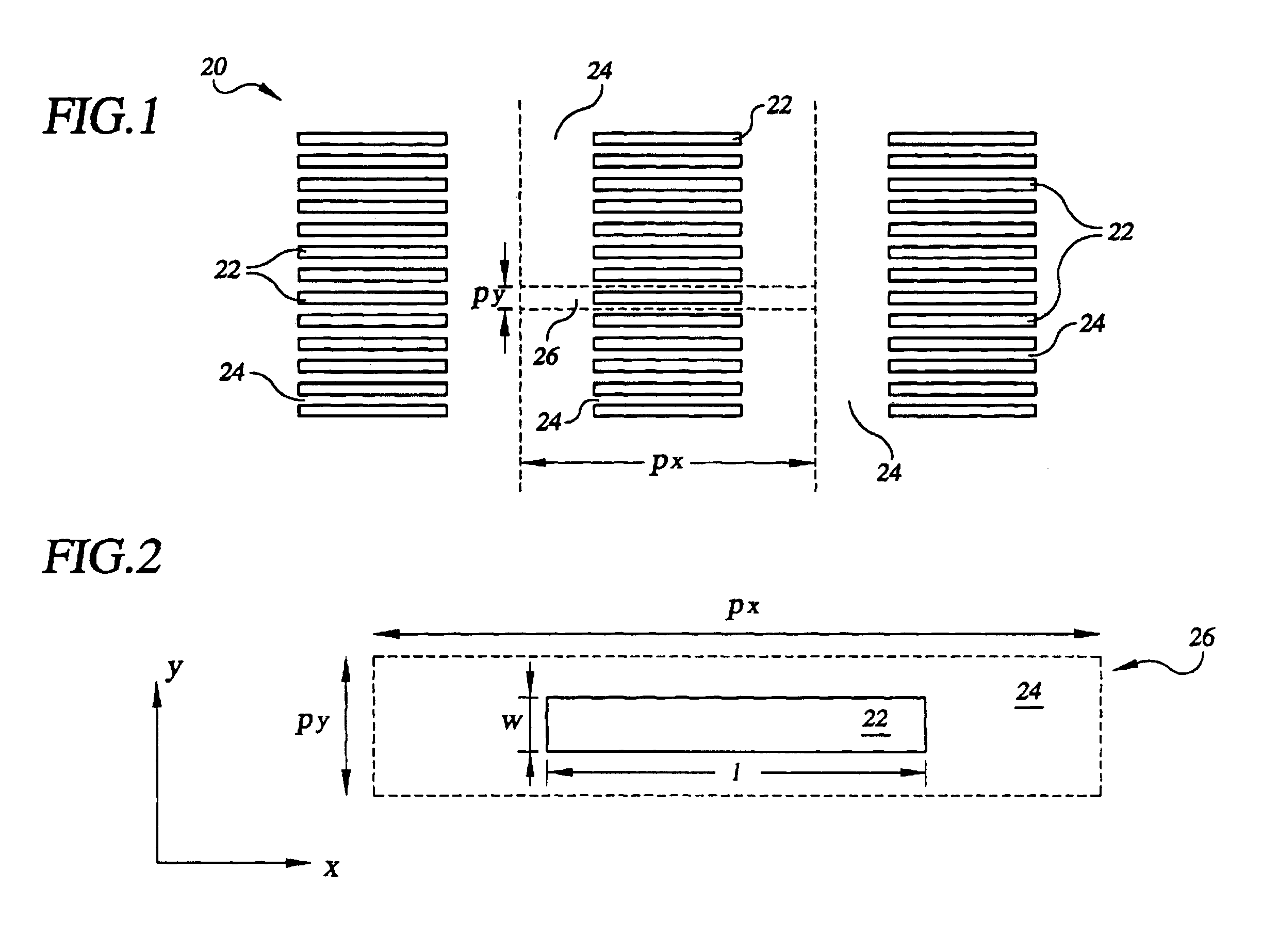
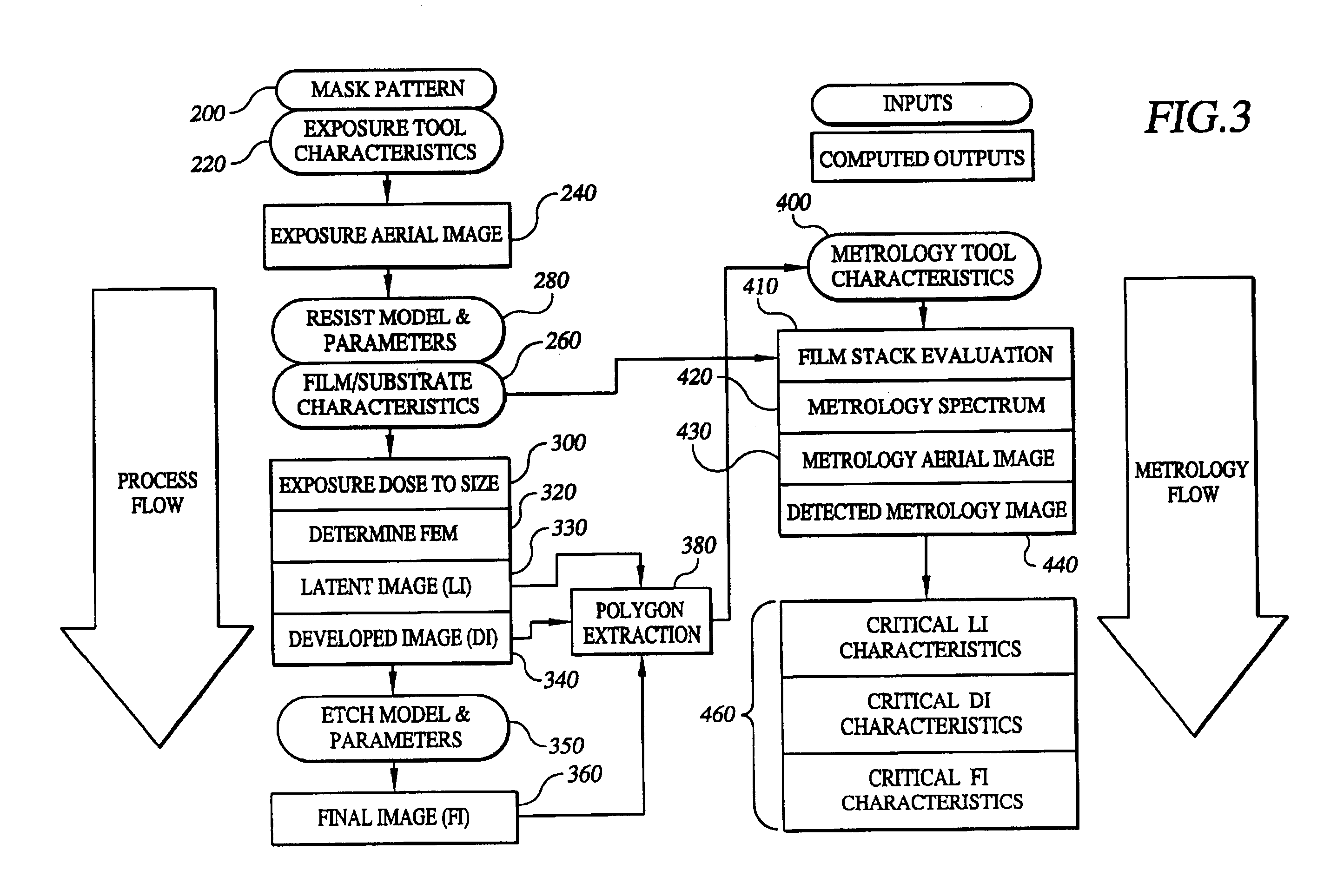
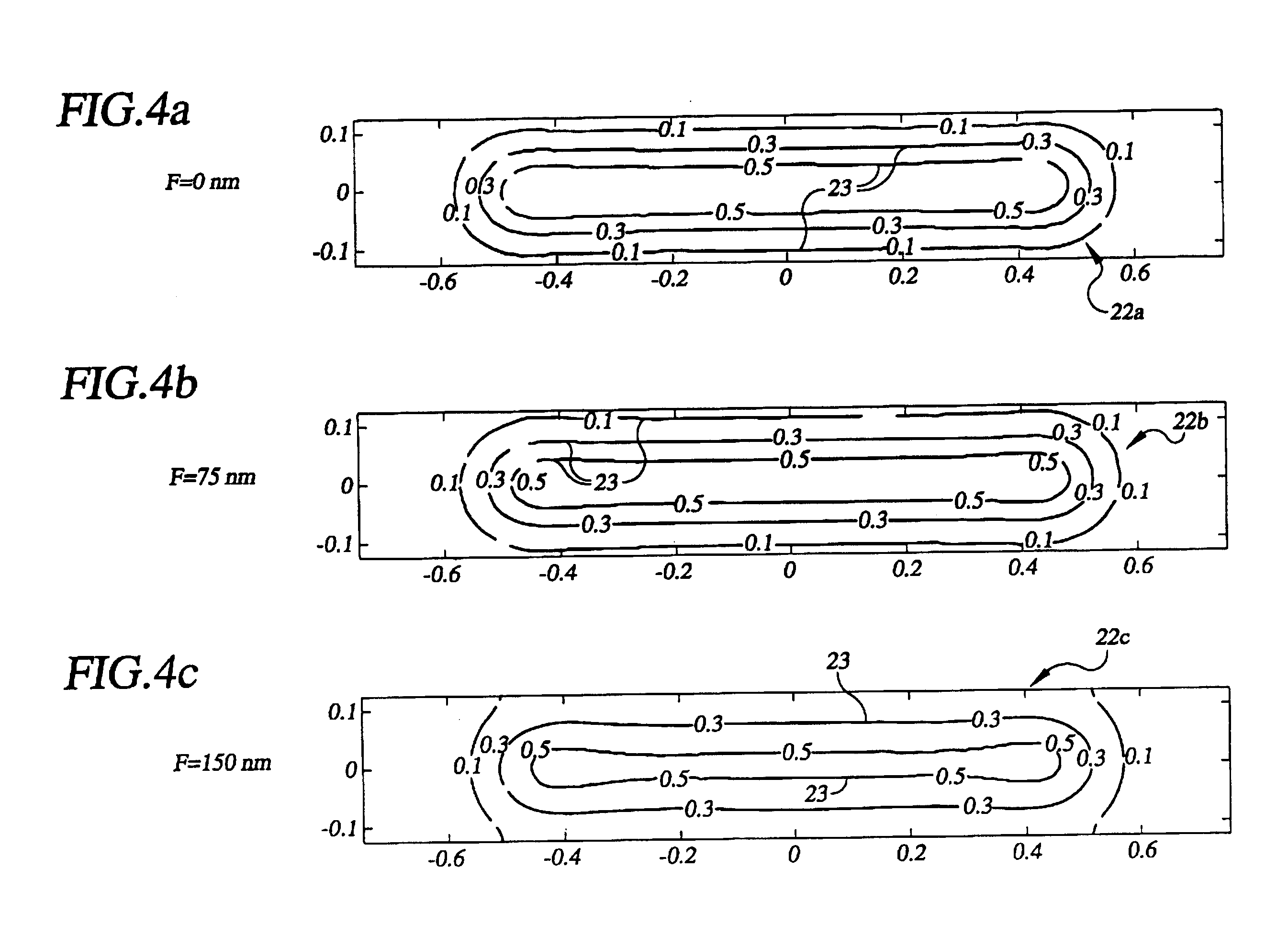
Optical metrology systems used to monitor exposure and dose, as well as other lithographic parameters, have been disclosed in the prior art, for example the bright field system disclosed in U.S. Pat. No. 6,130,750 (see FIG. 22) and the dark field system disclosed in U.S. Pat. No. 6,183,919 (see FIGS. 3A and 3B). The disclosures of these patents are hereby incorporated by reference. The present invention provides a more accurate physical model of an optical critical dimension (OCD) metrology system in a method and system that may be employed in a stand-alone software package. The model preferably works in essentially two stages. In the first stage, the aerial image intensity of the desired object, i.e., the target, is com...


PUM


Abstract

A method of modeling dose and focus response in lithographic imaging to simulate an optical critical dimension (OCD) metrology system creates simulated aerial images of the object pattern to be transferred to a resist film on the substrate at different focus settings of the metrology imaging system. The method then successively creates simulated images, at different exposure dose and focus settings of the metrology imaging system, of the latent and developed image of the object pattern in the resist film on the substrate, and the etched image of the object pattern in the substrate. The method converts the simulated images into polygons having more than four sides and determines the Fourier spectrum of the polygons simulating the images of the object pattern. Using the spectrum of the polygons simulating the images of the object pattern, the method then creates simulated aerial images of the object pattern developed in the resist film, at different dose and focus settings, as viewed by the OCD metrology system.

Description

BACKGROUND OF THE INVENTION1. Field of the InventionThis invention relates to lithographic processing of microelectronics products and, in particular, to a method and system for simulating an optical critical dimension metrology system used to evaluate the effects of dose and focus during lithographic processing2. Description of Related ArtLithographic processing to produce microelectronic circuits on semiconductor wafers requires, among other things, optimization of exposure dose and focus of the energy source used to expose the mast films. An optical critical dimension (OCD) metrology system evaluates dose and / or focus response in a lithographic imaging system by measuring the changes in a printed target, for example, the length of printed lines, in a focus / dose matrix.Conventional lithography simulators are designed to model the imaging of manhattan-type mask patterns onto the wafer. It has been found that conventional lithography simulators are inadequate in modeling an OCD metr...

Claims


Application Information

Patent Timeline
IPC IPC(8): G03F9/00G03F7/20
CPCG03F7/705G03F7/70666G03F7/70641G03F7/70625G03F7/70683
Inventor AUSSCHNITT, CHRISTOPHER P.GORDON, RONALD L.PROGLER, CHRISTOPHER J.ROSENBLUTH, ALAN E.
Owner GLOBALFOUNDRIES INC
Why Eureka
Try Eureka