High performance system-on-chip discrete components using post passivation process

a post-passivation process and discrete component technology, applied in the direction of semiconductor devices, semiconductor/solid-state device details, inductances, etc., can solve the problems of limiting the upper bound of the cut-off frequency that can be achieved for the inductor, and inability to meet the requirements of many applications, so as to improve the rf performance of high-performance integrated circuits

Inactive Publication Date: 2005-03-22
QUALCOMM INC
View PDF15 Cites 78 Cited by
  • Summary
  • Abstract
  • Description
  • Claims
  • Application Information

AI Technical Summary

Benefits of technology

It is the primary objective of the invention to improve t

Problems solved by technology

In creating an inductor on a monolithic substrate on which additional semiconductor devices are created, the parasitic capacitances that occur as part of this creation limit the upper bound of the cut-off frequency that can be achieved for the inductor using conventional silicon processes.
This limitation is, for many applications, not acceptable.
Prior Art has in this been limited to creating values of higher quality factors as separate units, and in integrating these separate units with the surrounding device functions.
The non-monolithic approach also has the disadvantage that additional wiring is required to interconnect the sub-components of the assembly, thereby again introducing additional parasitic capacitances and resistive losses over the interconnecting wiring network.
By raising the power consumption, the effects of parasitic capacitances and resistive power loss can be partially compensated, but there are limitations to even this approach.
These problems take on even greater urgency with the rapid expansion of wireless applications, such as portable telephones and the like.
Wireless communication is a rapidly expanding market, where the integration of RF integrated circuits is one of the most important challenges.
Where however more complex applications are required, the need still exists to create inductors using silicon as a

Method used


Image

  • High performance system-on-chip discrete components using post passivation process
  • High performance system-on-chip discrete components using post passivation process
  • High performance system-on-chip discrete components using post passivation process

Examples


Embodiment Construction

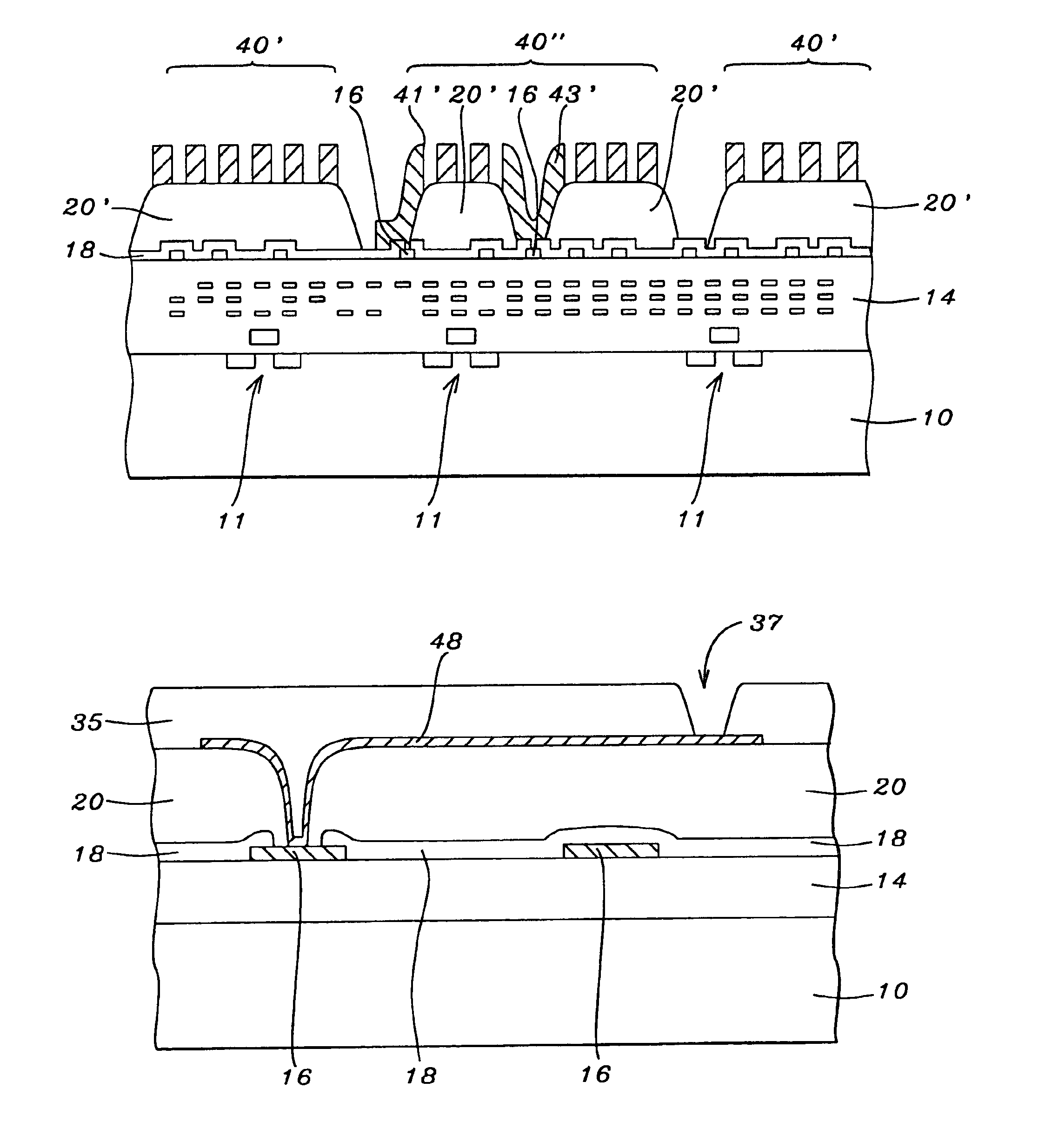
U.S. Pat. No. 6,383,916, assigned to a common assignee as the current invention, teaches an Integrated Circuit structure where re-distribution and interconnect metal layers are created in layers of dielectric over the passivation layer of a conventional Integrated Circuit (IC). A layer of passivation is deposited over the IC, a thick layer of polymer is alternately deposited over the surface of the layer of passivation, and thick, wide metal lines are formed over the passivation.

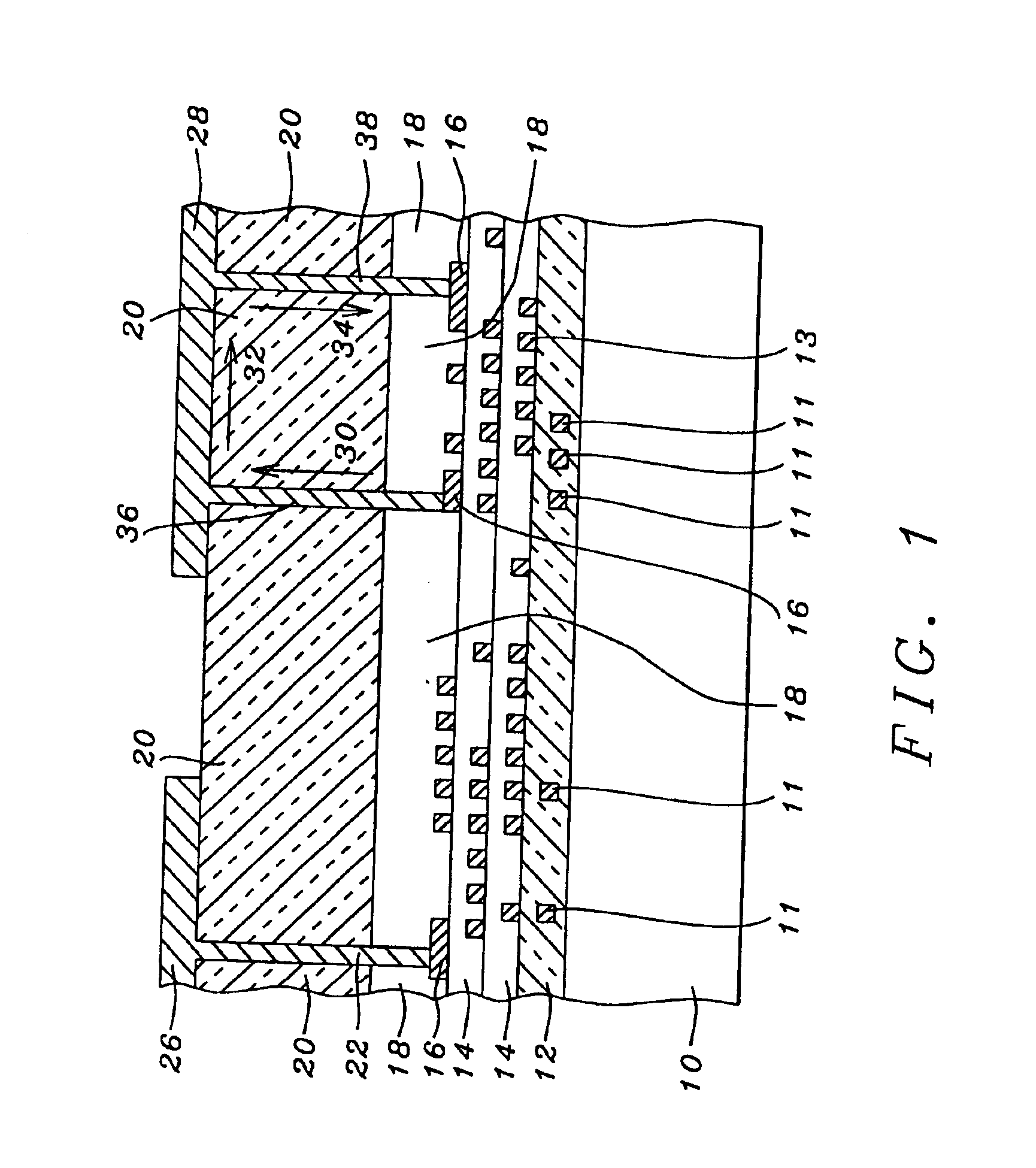
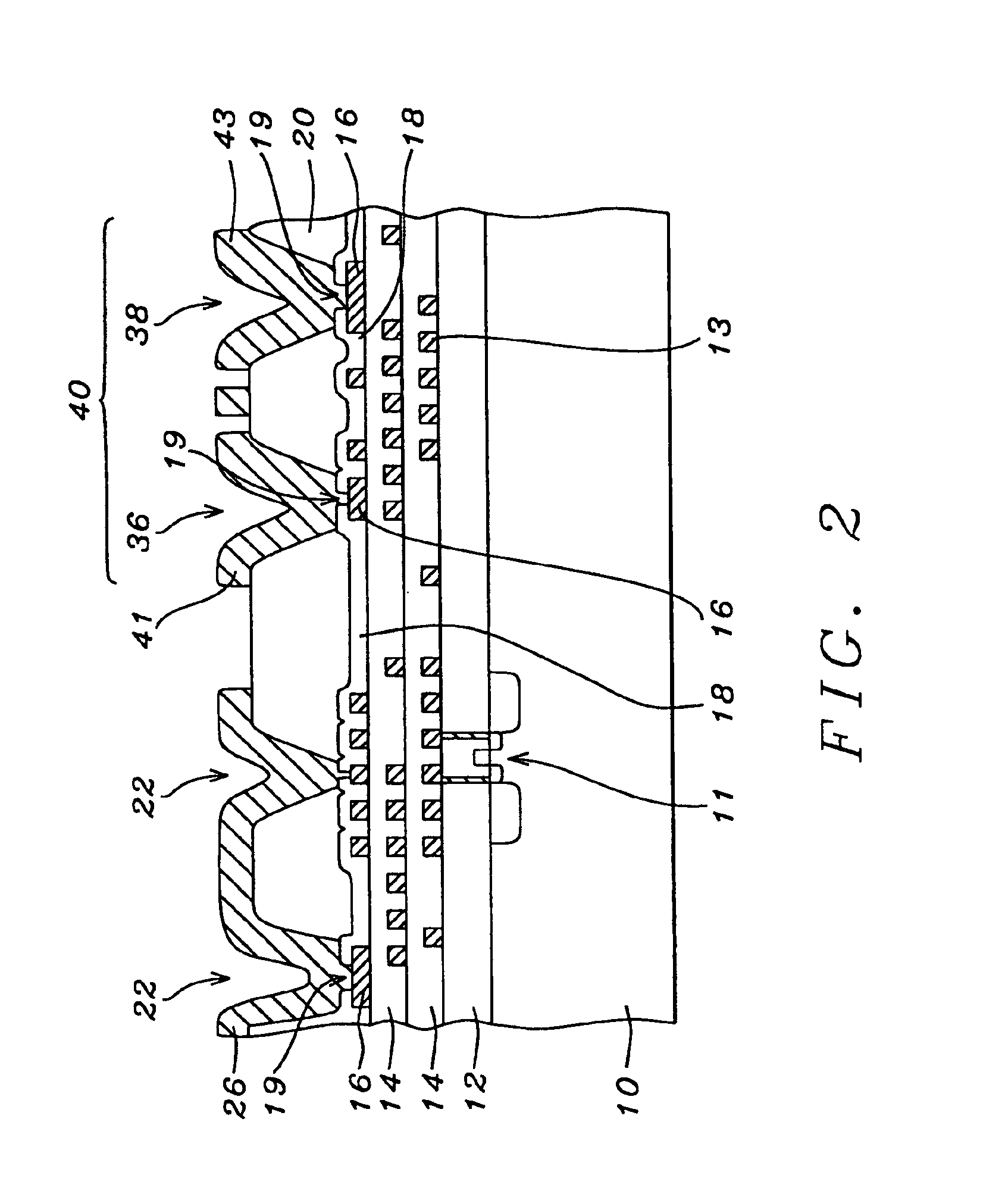
U.S. Pat. No. 6,303,423, also assigned to a common assignee as the current invention, addresses, among other objectives, the creation of an inductor whereby the emphasis is on creating an inductor of high Q value above the passivation layer of a semiconductor substrate. The high quality of the inductor of the invention allows for the use of this inductor in high frequency applications while incurring minimum loss of power. The invention further addresses the creation of a capacitor and a resistor on the surf...


PUM


Abstract

A system and method for forming post passivation discrete components, is described. High quality discrete components are formed on a layer of passivation, or on a thick layer of polymer over a passivation layer.

Description

BACKGROUND OF THE INVENTION(1) Field of the InventionThe invention relates to the manufacturing of high performance Integrated Circuit (IC's), and, more specifically, to methods of creating high performance electrical components (such as an inductor) on the surface of a semiconductor substrate by reducing the electromagnetic losses that are typically incurred in the surface of the substrate.(2) Description of the Related ArtThe continued emphasis in the semiconductor technology is to create improved performance semiconductor devices at competitive prices. This emphasis over the years has resulted in extreme miniaturization of semiconductor devices, made possible by continued advances of semiconductor processes and materials in combination with new and sophisticated device designs. Most of the semiconductor devices that are at this time being created are aimed at processing digital data. There are however also numerous semiconductor designs that are aimed at incorporating analog func...

Claims


Application Information

Patent Timeline
IPC IPC(8): H01L23/52H01L21/70H01L23/522H01L21/02H01L23/64H01L23/58H01L23/60H01L23/532H01L21/768H01L23/528H01L27/06H01L27/08
CPCH01L23/522H01L23/5222H01L23/5223H01L23/5227H01L23/5228H01L23/5286H01L23/5329H01L23/60H01L23/642H01L23/645H01L23/647H01L24/03H01L24/05H01L24/11H01L27/0676H01L27/08H01L28/10H01L28/20H01L2224/0401H01L2224/13022H01L2224/45124H01L2224/45144H01L2924/01006H01L2924/01011H01L2924/01013H01L2924/01014H01L2924/01022H01L2924/01028H01L2924/01029H01L2924/01038H01L2924/01042H01L2924/01047H01L2924/0105H01L2924/01073H01L2924/01074H01L2924/01075H01L2924/01078H01L2924/01079H01L2924/01082H01L2924/014H01L2924/04941H01L2924/04953H01L2924/05042H01L2924/10329H01L2924/14H01L2924/1423H01L2924/15174H01L2924/19015H01L2924/19041H01L2924/19042H01L2924/19043H01L2924/19104H01L2924/30105H01L2924/3011H01L2924/3025H01L2224/05H01L24/45H01L2924/01005H01L2924/01019H01L2924/01024H01L2924/01033H01L23/3192H01L2224/04042H01L2924/10253H01L2924/00014H01L2924/00H01L2224/48H01L24/02H01L24/13H01L24/16H01L2224/02311H01L2224/02313H01L2224/0345H01L2224/03462H01L2224/0347H01L2224/0361H01L2224/03914H01L2224/05082H01L2224/05083H01L2224/05548H01L2224/1132H01L2224/11334H01L2224/1146H01L2224/11849H01L2224/131H01L2224/16265H01L2224/29124H01L2224/29144H01L2224/29147H01L2224/29155H01L2224/29166H01L2224/29171H01L2224/2919H01L2224/81191H01L2224/05644H01L2224/05144H01L2224/05166H01L2224/05647H01L2224/05147H01L2224/05171H01L2224/05655
Inventor LIN, MOU-SHIUNG
Owner QUALCOMM INC
Why Eureka
Try Eureka