Light-emitting devices utilizing nanoparticles

a technology of light-emitting devices and nanoparticles, which is applied in the direction of discharge tubes/lamp details, discharge tubes luminescnet screens, electric discharge lamps, etc., can solve the problems of unsatisfactory applications requiring efficient generation of light at particular wavelengths, the efficiency with which light may be extracted from such devices is reduced, and the loss due to total internal reflection increases rapidly. , to achieve the effect of reducing light scattering, increasing light extraction, and increasing light extraction

Inactive Publication Date: 2005-03-22
LUMILEDS
View PDF7 Cites 169 Cited by
  • Summary
  • Abstract
  • Description
  • Claims
  • Application Information

AI Technical Summary

Benefits of technology

The light-emitting devices disclosed herein may advantageously exhibit increased light extraction from a primary light source, increased lig

Problems solved by technology

A common problem with conventional semiconductor light-emitting devices is that the efficiency with which light may be extracted from such a device is reduced by total internal reflection at interfaces between the device and the surrounding environment followed by reabsorption of the reflected light in the device.
Losses due to total internal reflection increase rapidly with the ratio of the refractive index inside the device to that outside the device.
Another aspect of conventional semiconductor light-emitting devices which may be disadvantageous for some applications is that the emission spectrum of such a device typically exhibits a single rather narrow peak (full width at half maximum

Method used


Image

  • Light-emitting devices utilizing nanoparticles
  • Light-emitting devices utilizing nanoparticles
  • Light-emitting devices utilizing nanoparticles

Examples


Embodiment Construction

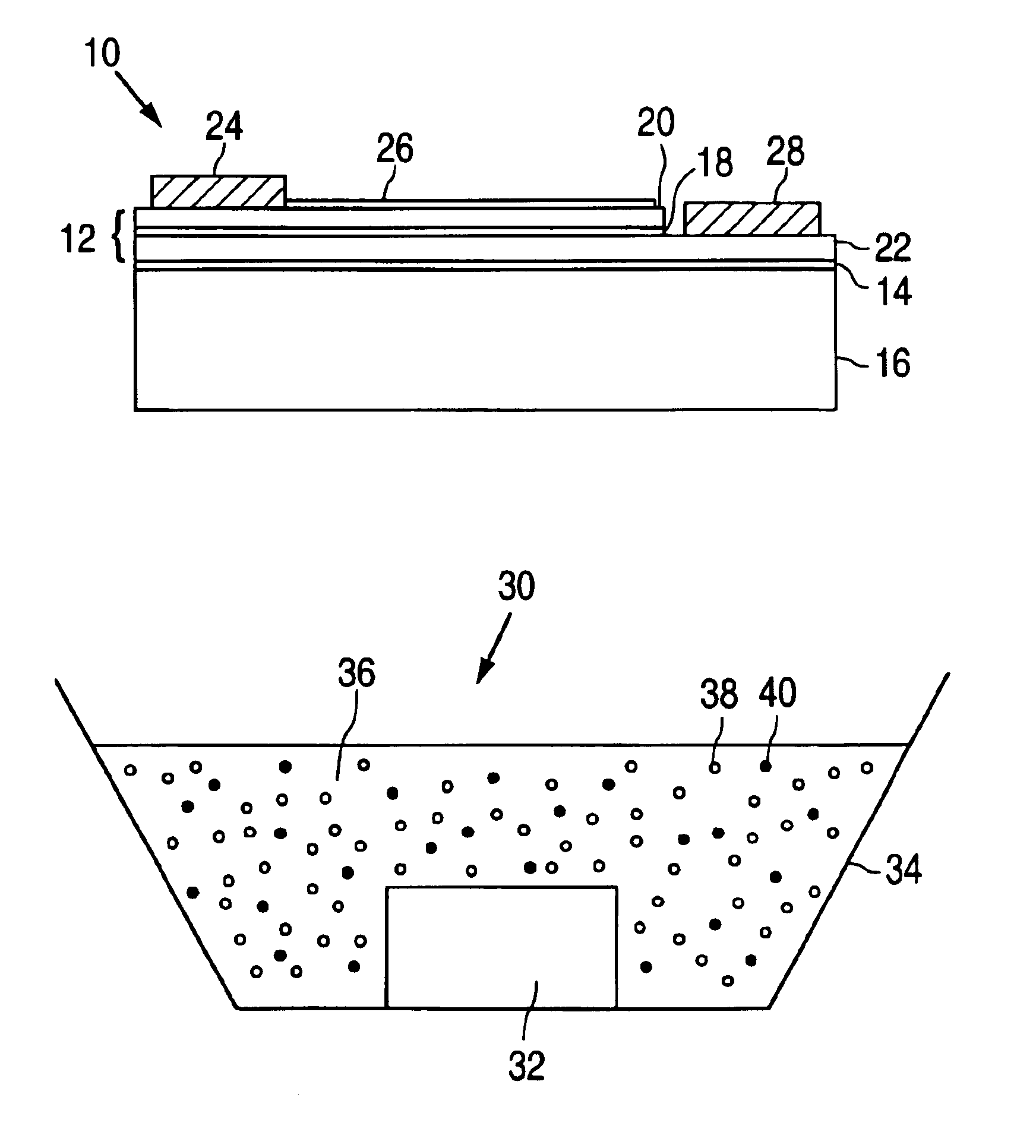
Several embodiments of light-emitting devices are disclosed in which nanoparticles are used in combination with light-emitting semiconductor devices. As used herein, “nanoparticle” refers to a particle having a diameter (or similar cross-sectional dimension) typically much less than about one micron. Such nanoparticles may be of any shape and may comprise, for example, crystalline or amorphous solids or liquids.

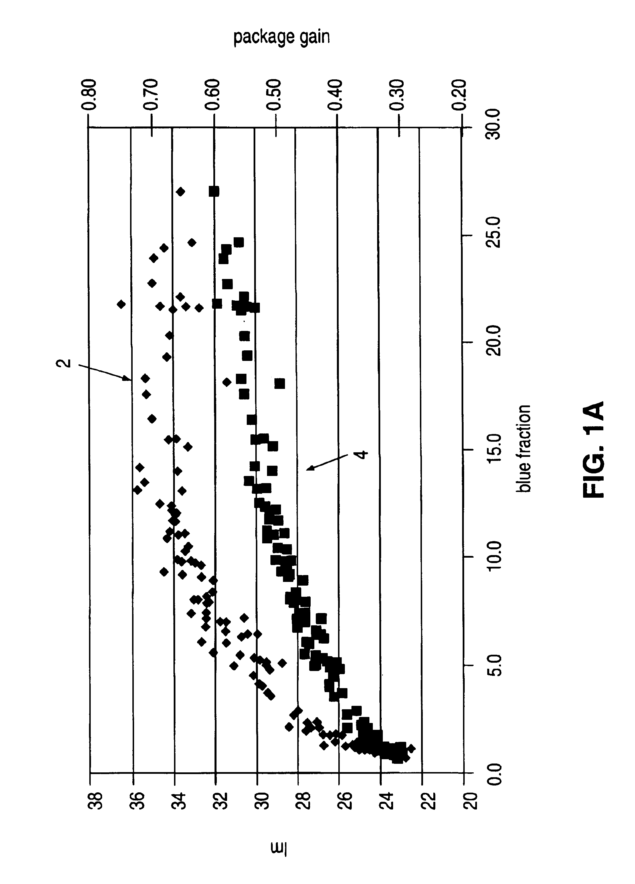
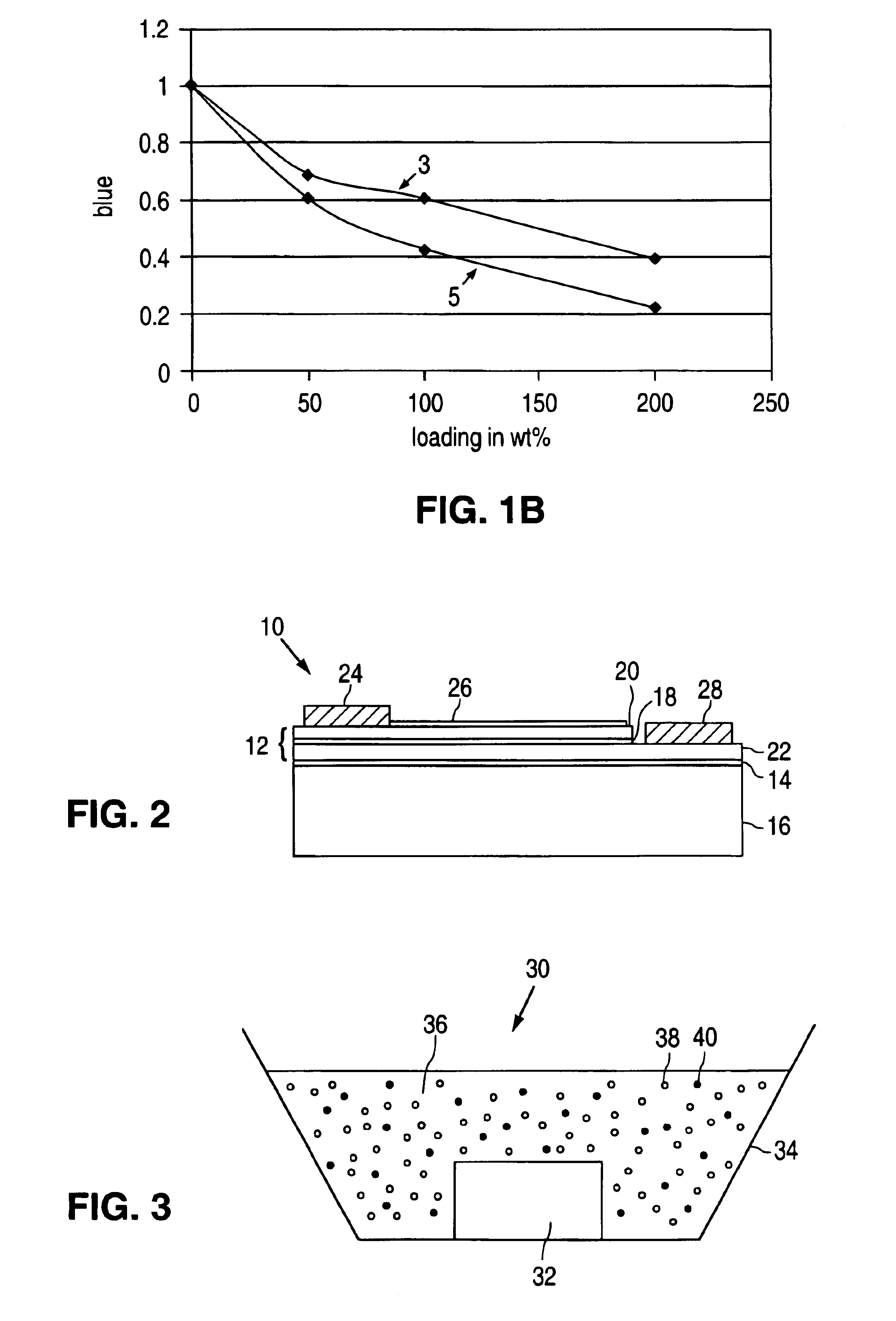
The inventors have discovered that the efficiency of conventional phosphor-converted light-emitting devices is significantly decreased by scattering by the phosphor particles of both the primary emission from the semiconductor device and the secondary emission from the phosphor particles. A portion of the light scattered by the phosphor particles is scattered onto absorbing parts of the semiconductor device or its package and thereby lost.

Such scattering by the phosphor particles occurs because they are typically substantially larger than the wavelengths of the primary and se...


PUM


Abstract

Light-emitting devices are disclosed that comprise a light source emitting first light, a first material substantially transparent to and located to receive at least a portion of the first light, and particles of a second material dispersed in the first material. The second material has an index of refraction greater than an index of refraction of the first material at a wavelength of the first light. The particles of the second material have diameters less than about this wavelength. Particles of a third material may also be dispersed in the first material.

Description

FIELD OF THE INVENTIONThe present invention relates to light-emitting devices, and more particularly to semiconductor light-emitting devices.BACKGROUNDSemiconductor light-emitting devices such as light-emitting diodes (LEDs) and laser diodes (LDs) are among the most efficient and robust light sources currently available. Material systems currently of interest in the manufacture of high brightness LEDs capable of operation across the visible spectrum include group III-V semiconductors, particularly binary, ternary, and quaternary alloys of gallium, aluminum, indium, and nitrogen, also referred to as III-nitride materials, and binary, ternary, and quaternary alloys of gallium, aluminum, indium, and phosphorus, also referred to as III-phosphide materials.A common problem with conventional semiconductor light-emitting devices is that the efficiency with which light may be extracted from such a device is reduced by total internal reflection at interfaces between the device and the surrou...

Claims


Application Information

Patent Timeline
IPC IPC(8): H01L33/00H01L33/50H01L33/56
CPCH01L33/501H01L33/56H01L2933/0091
Inventor MUELLER, GERD O.MUELLER-MACH, REGINA B.BERTRAM, DIETRICHJUESTEL, THOMASSCHMIDT, PETER J.OPITZ, JOACHIM
Owner LUMILEDS
Why Eureka
Try Eureka