Method of making a semiconductor chip assembly with a conductive trace and a substrate

a technology of semiconductor chips and trace, applied in the field of semiconductor chip assemblies, can solve the problems of significant cost and technical limitations, overall cost saving, and significant cost of forming bumps on the pads, and achieve the effects of low cost, high reliability and high performan

Inactive Publication Date: 2005-03-29
BRIDGE SEMICON
View PDF149 Cites 23 Cited by
  • Summary
  • Abstract
  • Description
  • Claims
  • Application Information

AI Technical Summary

Benefits of technology

[0019]An object of the present invention is to provide a semiconductor chip assembly with a chip, a conductive trace and a substrate that provides a low cost, high is performance, high reliability package.
[0020]Another object of the present invention is to provide a convenient, cost-effective method for manufacturing semiconductor chip assemblies as grid arrays or other structures.

Problems solved by technology

In addition, flip-chip bonding requires minimal mounting area and weight which results in overall cost saving since no extra packaging and less circuit board space are used.
While flip-chip technology has tremendous advantages over wire bonding and TAB, its cost and technical limitations are significant.
For instance, the cost of forming bumps on the pads is significant.
In addition, an adhesive is normally underfilled between the chip and the support circuit to reduce stress on the solder joints due to thermal mismatch between the chip and the support circuit, and the underfilling process increases both manufacturing complexity and cost.
Finally, the solder is typically a tin-lead alloy and lead-based materials are becoming far less popular due to environmental concerns over disposing of toxic materials and leaching of toxic materials into ground water supplies.
Drawbacks to this approach include complicated manufacturing requirements, high cost, and chip loss if the additional circuitry is defective.
In particular, since the chip or wafer provides a substrate for the additional circuitry, chips will be lost if the additional circuitry fails to achieve certain quality and yield criteria.
Unpredictable chip loss has prevented the wide spread adoption of this “chip first” approach in volume production.
Furthermore, if the process is not performed on wafers, the commercially available silicon wafer processing equipment may not be compatible with common tooling and handling techniques.
However, advanced logic chips such as microprocessors, digital signal processors (DSP) and application-specific integrated circuits (ASIC) often require the package to be considerably larger than the chip to accommodate high pin counts and meet motherboard pitch limitations.
Unfortunately, these larger packages often employ wire bonding, TAB or flip-chip bonding, and as mentioned above, these connection techniques are not entirely satisfactory.
However, the BBUL package has the disadvantages mentioned above for thin film routing.
Namely, complicated manufacturing requirements, high cost, and chip loss if the additional circuitry is defective.
Furthermore, the BBUL package does not route the pads to the back-side of the substrate.

Method used


Image

  • Method of making a semiconductor chip assembly with a conductive trace and a substrate
  • Method of making a semiconductor chip assembly with a conductive trace and a substrate
  • Method of making a semiconductor chip assembly with a conductive trace and a substrate

Examples


Embodiment Construction

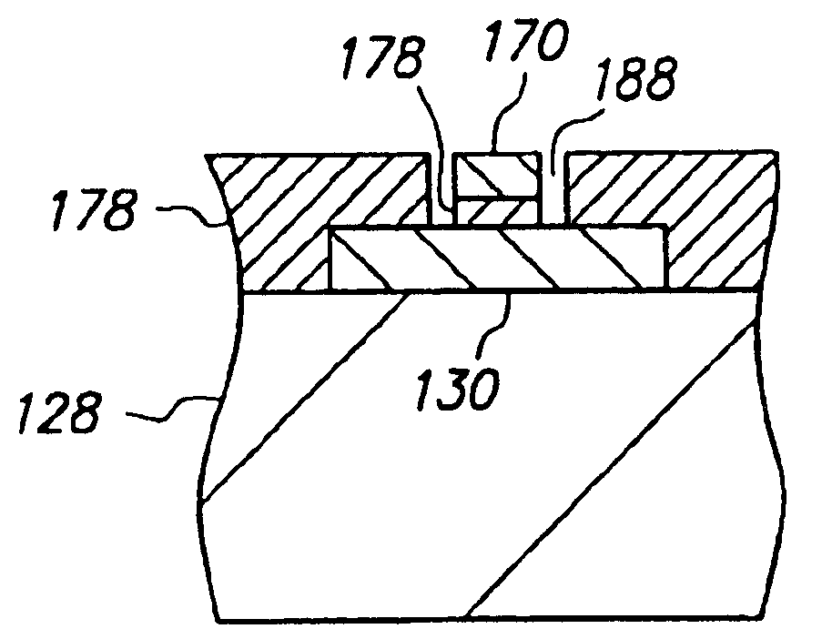
[0132]FIGS. 1A-14A, 1B-14B and 1C-14C are cross-sectional, top and bottom views, respectively, of a method of making a semiconductor chip assembly in accordance with a first embodiment of the present invention.

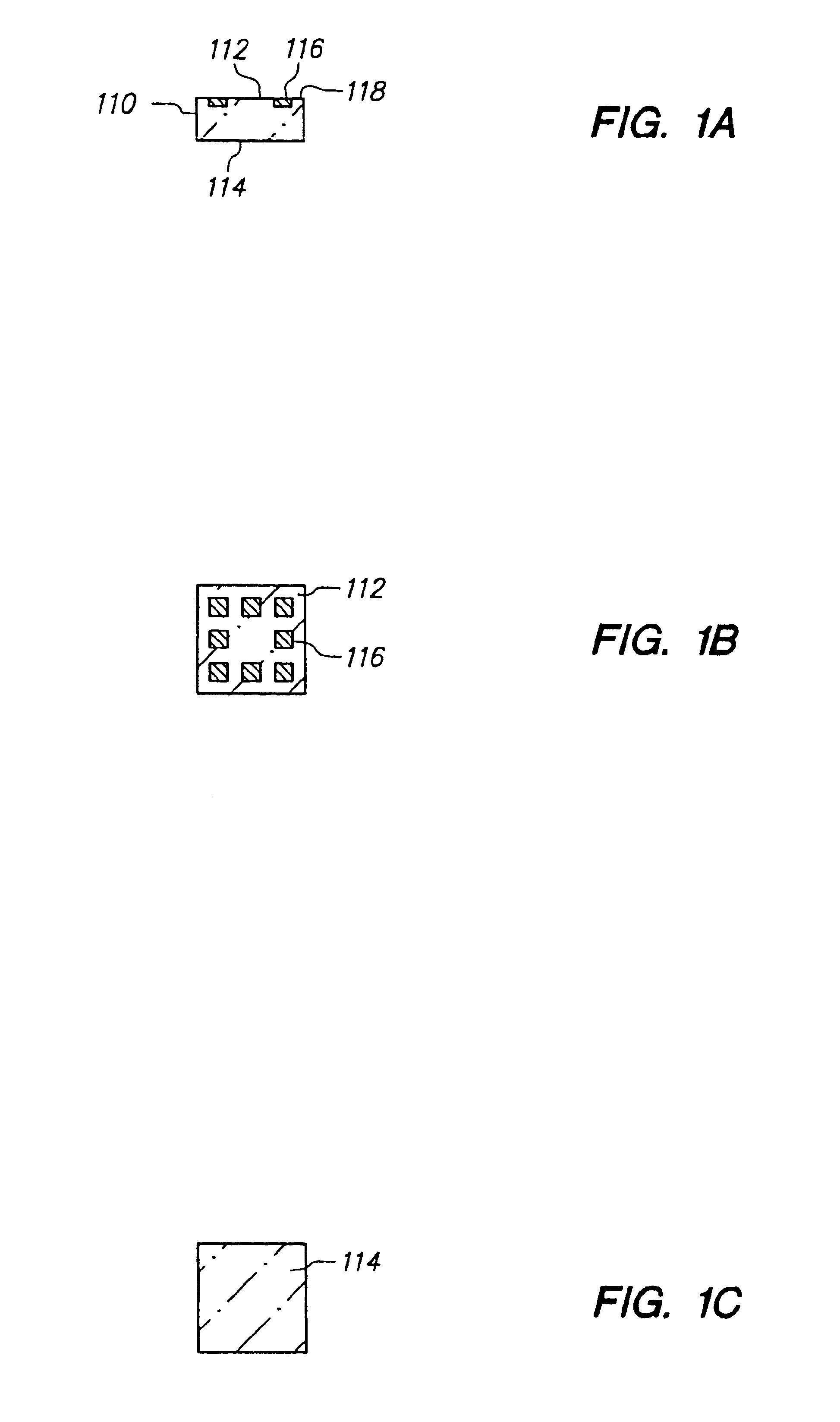
[0133]FIGS. 1A, 1B and 1C are cross-sectional, top and bottom views, respectively, of semiconductor chip 110 which is an integrated circuits in which various transistors, circuits, interconnect lines and the like are formed (not shown). Chip 110 includes opposing major surfaces 112 and 114, conductive pad 116 and passivation layer 118. Chip 110 has a length and width across surfaces 112 and 114 of 10 millimeters, and a thickness between surfaces 112 and 114 of 350 microns. Surface 112 is the active surface and includes pad 116 and passivation layer 118.

[0134]Pad 116 is substantially aligned with passivation layer 118 so that surface 112 is essentially flat. Alternatively, if desired, pad 116 can extend above or be recessed below passivation layer 118. Pad 116 provides a bondin...


PUM

PropertyMeasurementUnit
thicknessaaaaaaaaaa
thicknessaaaaaaaaaa
widthaaaaaaaaaa

Abstract

A method of making a semiconductor chip assembly includes providing a semiconductor chip, a conductive trace and a substrate, wherein the chip includes first and second opposing major surfaces and a conductive pad, the pad extends to the first surface of the chip, the substrate includes first and second opposing major surfaces, a conductive terminal and a dielectric base, the conductive terminal extends through the dielectric base to the first and second surfaces of the substrate, a cavity extends from the first surface of the substrate into the substrate, the first surfaces of the chip and the substrate face in a first direction, the second surfaces of the chip and the substrate face in a second direction, and the chip extends into the cavity, and then electrically connecting the conductive terminal to the pad using the conductive trace.

Description

CROSS-REFERENCE TO RELATED APPLICATIONS[0002]This application is a continuation-in-part of U.S. application Ser. No. 09 / 962,754 filed Sep. 24, 2001, now U.S. Pat. No. 6,673,710, which is a continuation-in-part of U.S. application Ser. No. 09 / 878,626 filed Jun. 11, 2001, now U.S. Pat. No. 6,653,217, which is a continuation-in-part of U.S. application Ser. No. 09 / 687,619 filed Oct. 13, 2000, now U.S. Pat. No. 6,440,835, each of which is incorporated by reference.BACKGROUND OF THE INVENTION[0003]1. Field of the Invention[0004]The present invention relates to a semiconductor chip assembly, and more is particularly to a semiconductor chip assembly that includes a semiconductor chip, a conductive trace and a substrate and its method of manufacture.[0005]2. Description of the Related Art[0006]Semiconductor chips have input / output pads that must be connected to external circuitry in order to function as part of an electronic system. The connection media is typically an array of metallic lea...

Claims


Application Information

Patent Timeline
Patent Type & Authority Patents(United States)
IPC IPC(8): H01L21/48H01L23/31H05K3/40
CPCH01L21/4853H01L23/3114H01L23/3128H01L2224/1134H01L2924/01012H01L2924/01013H01L2924/01029H01L2924/0103H01L2924/01079H01L2924/01082H01L2924/09701H01L2924/1433H01L2924/19041H01L2924/3011H01L2924/3025H05K3/4046H01L2924/01005H01L2924/01006H01L2924/01019H01L2924/01024H01L2924/01033H01L2924/0104H01L2924/01047H01L2924/01074H01L2924/01087H01L2924/01327H01L2224/45124H01L2224/45144H01L24/82H01L2224/05624H01L2924/10253H01L2924/00014H01L2924/30107H01L2224/48624H01L2224/0401H01L2224/48724H01L2924/181H01L2924/14H01L2924/3511H01L2924/3512H01L2224/19H01L2224/04105H01L2224/24227H01L2924/18162H01L21/568H01L2924/00H01L2924/00015H01L2224/48H01L2224/18H01L2924/00012
Inventor WANG, CHIA-CHUNGLIN, CHARLES W. C.
Owner BRIDGE SEMICON
Why Eureka
Try Eureka