Method of forming a memory cell with a single sided buried strap

a memory cell and buried strap technology, applied in the direction of basic electric elements, electrical equipment, semiconductor devices, etc., can solve the problems of reducing device reliability, leakage problem, unsuitable for use in narrower trench process, etc., and achieve the effect of reducing ic size and ameliorating disadvantages

Active Publication Date: 2005-03-29
NAN YA TECH
View PDF9 Cites 14 Cited by
  • Summary
  • Abstract
  • Description
  • Claims
  • Application Information

AI Technical Summary

Benefits of technology

The present invention improves on the prior art in that the angle implantation with fluorine-containing ions causes the first oxide layer on the first sidewall to be greater than the second oxide layer on the second sidewall. The second oxide layer is removed to expose the second sidewall, the first oxide layer, however, remains on the first sidewall. A single sided buried strap is then formed at the bottom of the opening. Thus, the single sided buried strap is insulated from the first sidewall by the first oxide layer, thereby solving the leakage problem between adjacent source regions. In addition, the present invention is well suited to the 0.11 μm (or below) trench technology, thereby achieving the goal of reduction in IC size and ameliorating the disadvantages of the prior art.

Problems solved by technology

The gap created between adjacent source regions causes a serious leakage problem (also referred to as a buried strap mergence issue), reducing device reliability.
Thus, the leakage problem occurs when the design rule is below 0.11 μm.
Nevertheless, this method suffers from misalignment issue during photolithography, making it unsuitable suitable for use in the narrower trench process.

Method used


Image

  • Method of forming a memory cell with a single sided buried strap
  • Method of forming a memory cell with a single sided buried strap
  • Method of forming a memory cell with a single sided buried strap

Examples


an embodiment

according to the present invention will be explained with reference to FIGS. 2A˜2J.

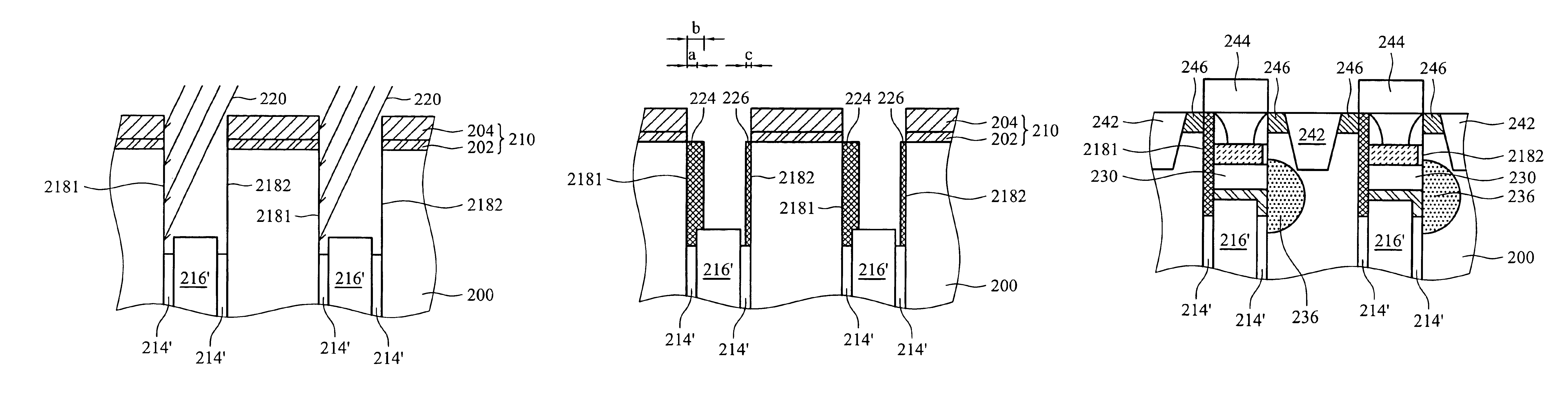
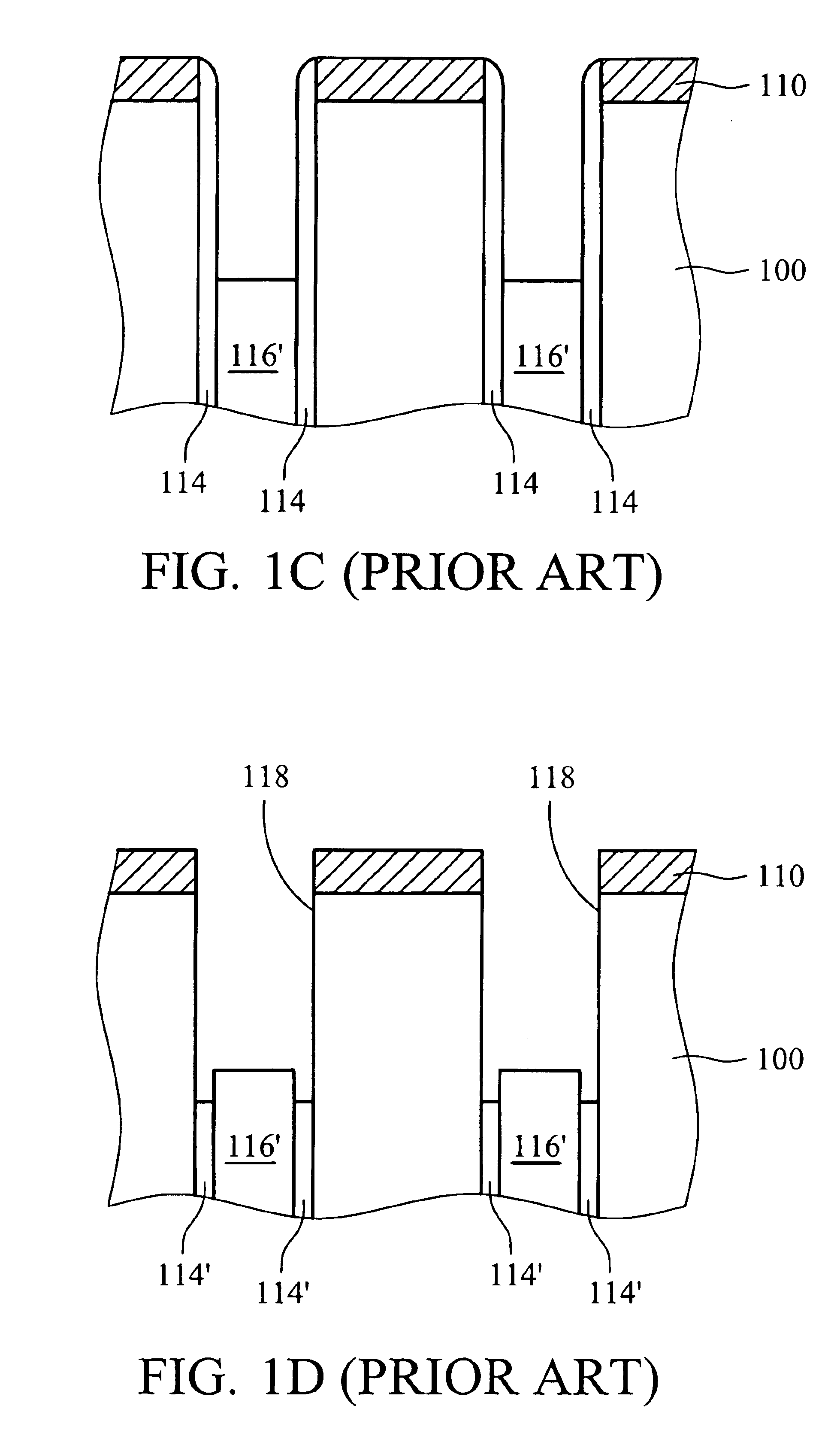
In FIG. 2A, a semiconductor substrate 200 is provided. The semiconductor substrate 200 is composed of silicon or germanium. The semiconductor substrate 200 can be made by epitaxial silicon or silicon on insulator. For simplicity, a P-type semiconductor silicon substrate 200 is given as an example in this invention. A patterned pad layer 210 composed of a pad oxide layer (such as SiO2) 202 and a silicon nitride layer 204 (such as Si3N4) is formed on part of the substrate 200. The pad oxide layer 202 can be formed by oxidation and the silicon nitride layer 204 can be formed by CVD (chemical vapor deposition). The thickness of the pad layer 210 is about 1500 to 3000 Å. Using the pad layer 210 as a mask, part of the substrate 200 is removed to form a deep trench 212 therein. A trench capacitor (not shown) is then formed at the lower portion of the deep trench 212 by conventional processes, as disclosed in...


PUM


Abstract

A method of forming a memory cell with a single sided buried strap. A collar oxide layer is formed on the sidewall of a trench. A conductive layer fills the trench. The conductive layer and the collar oxide layer are partially removed to form an opening having first and second sidewalls. The remaining collar oxide layer is lower than the remaining conductive layer. An angle implantation with F ions is performed on the first sidewall. A thermal oxidation process is performed to form a first oxide layer on the first sidewall and a second oxide layer on the second sidewall. The first oxide layer is thicker than the second oxide layer. The second oxide layer is removed to expose the second sidewall. A buried strap is formed at the bottom of the opening, insulated from the first sidewall by the first oxide layer.

Description

BACKGROUND OF THE INVENTION1. Field of the InventionThe present invention relates to a method of fabricating a memory cell with a transistor, and more particularly, to a method of forming a dynamic random access memory (DRAM) cell having a single sided buried strap.2. Description of the Related ArtA DRAM cell comprises a metal-oxide-semiconductor field effect transistor (MOSFET) and a capacitor formed in a semiconductor silicon substrate. There is an electrical contact between the drain of a MOSFET and the bottom storage electrodes of the adjacent capacitor, which forms a memory cell of the DRAM device. A large number of memory cells make up the cell arrays which combine with the peripheral circuit to produce DRAMs.In recent years, MOSFET size has been continuously reduced so that the packing density of DRAM devices has increased considerably. For example, new techniques for manufacturing extremely small transistor elements have been developed for 1 Giga bit DRAMs and beyond. One of...

Claims


Application Information

Patent Timeline
Patent Type & Authority Patents(United States)
IPC IPC(8): H01L21/70H01L21/20H01L21/02H01L21/8242
CPCH01L27/10867H01L27/10864H10B12/0383H10B12/0385
Inventor HSIAO, CHIH-YUANCHEN, YI-NAN
Owner NAN YA TECH
Why Eureka
Try Eureka