
Inhomogeneous materials having physical properties decoupled from desired functions

a technology of physical properties and homogeneous materials, applied in the field of homogeneous materials, can solve the problems of insufficient thermal and mechanical stability of k materials, power dissipation, and insufficient future circuits

Inactive Publication Date: 2005-03-29
NOVELLUS SYSTEMS
View PDF15 Cites 34 Cited by
  • Summary
  • Abstract
  • Description
  • Claims
  • Application Information

AI Technical Summary

Benefits of technology

The invention provides a composition that can be cured to form a material with specific physical properties determined by a second component. The first component provides a response to radiation, which can be separately optimized. The resulting material can have low dielectric constant and can be used in metal interconnect layers in integrated circuits. The composition can be deposited as a layer on a substrate and then patterned using a radiation pattern. The photosensitive binder can bind or release the particles, resulting in the desired material properties.

Problems solved by technology

As the distances between the circuit elements become smaller, there will be increased problems due to capacitive coupling (crosstalk) and propagation delay, and to increased power dissipation associated with charge depletion from higher capacitance elements.
However, the dielectric constants of these materials range from 3.0-7.0 and thus will not be adequate for future circuits.
However, these low k materials have not been shown to have sufficient thermal and mechanical stability to survive the heat and mechanical stresses occurring during IC fabrication In addition, these polymers typically have chemical properties that are similar in some respects to the chemical properties of photoresist materials commonly used in IC fabrication.
Thus, selective chemical removal of photoresist layers deposited on layers of these low k materials might be difficult or impossible.
A problem with Kikkawa's approach, however, is that an MSQ film created in this manner might be weaker than a directly applied and conventionally patterned MSQ film as a result, for example, of component evaporation that weakens the film.
An additional problem with this approach is that the photo-patternability function of Kikkawa's film is not separated from the physical properties of the film.
Consequently, it may be difficult to separately optimize, for example, the photo-patternability, dielectric constant, and strength of the final MSQ film.
Another problem with Kikkawa's approach is that the dielectric constant of MSQ is typically in the range of 2.5 to 3.0, which is higher than the values of 1.0 to 2.2 desired by the semiconductor industry.
A general problem with such homogenous media is that their physical properties are often affected when new functions are engineered into the media.

Method used


Image

  • Inhomogeneous materials having physical properties decoupled from desired functions
  • Inhomogeneous materials having physical properties decoupled from desired functions
  • Inhomogeneous materials having physical properties decoupled from desired functions

Examples


example 1

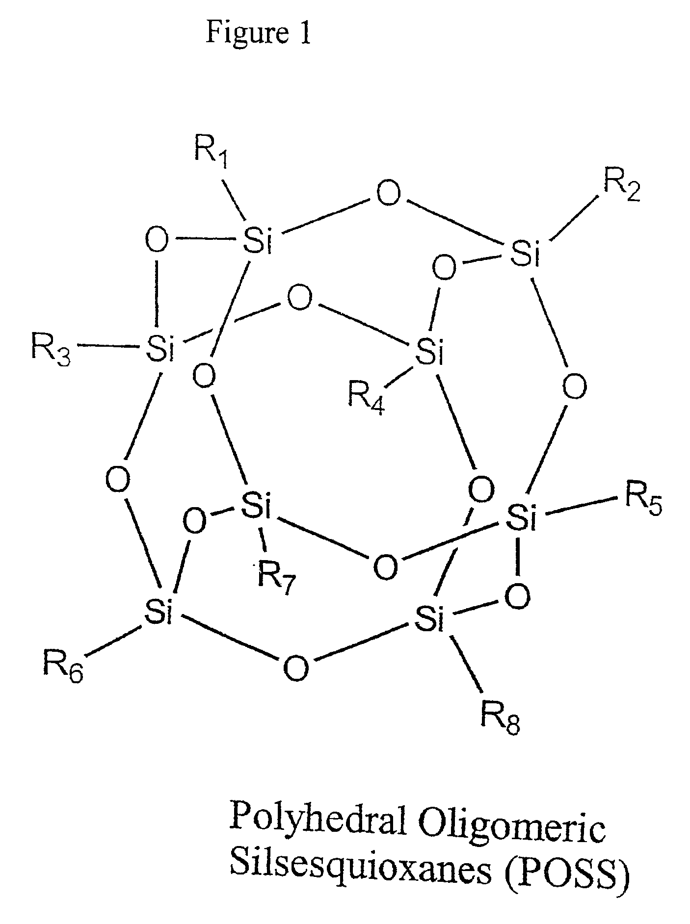
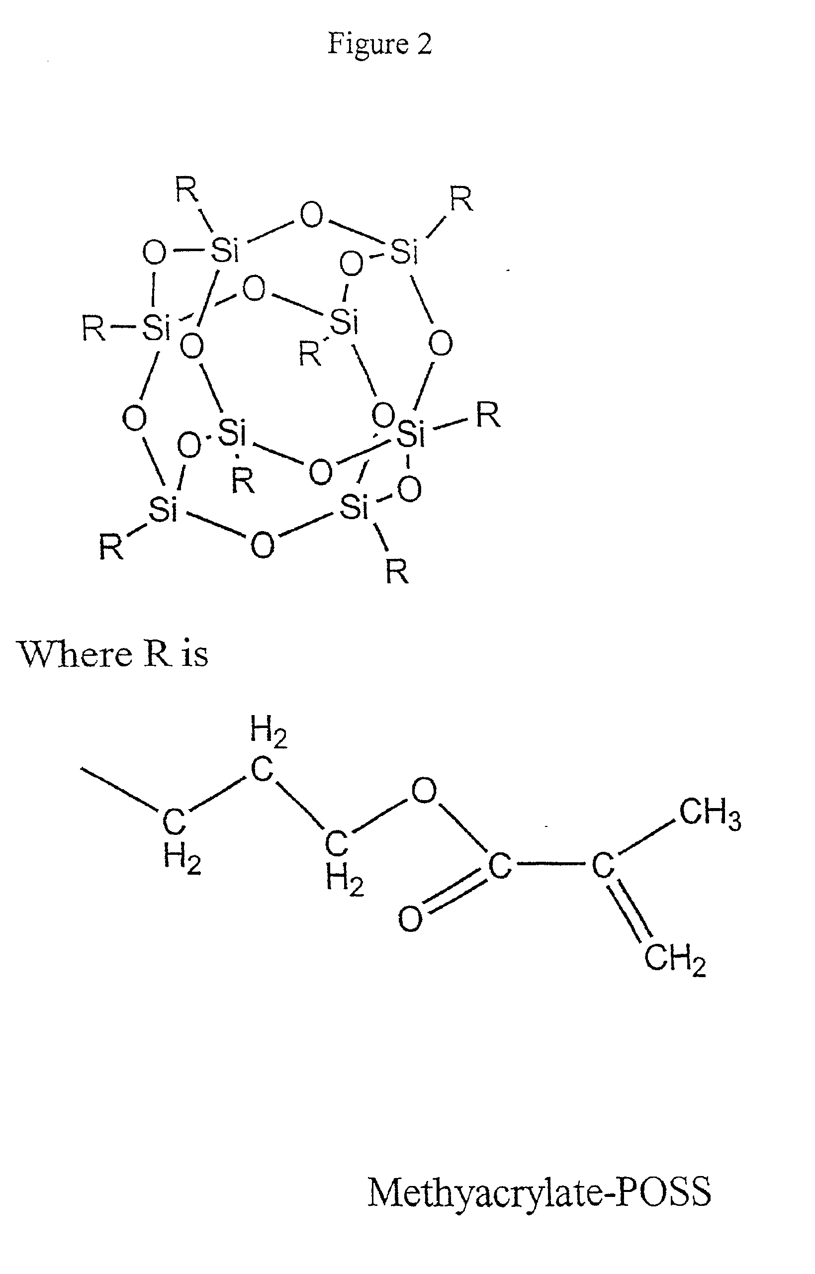
A colloidal suspension of silicalite crystals (having average diameters of about 300 Å to about 400 Å) in 1-propanol was prepared. The 8-fold substituted methacrylate-POSS discussed above was added to the colloidal suspension to a concentration of about 7.3 milligrams / milliliter (mg / ml). The mixture of silicalite and methacrylate-POSS was sonicated for about three hours (in a series of ½ hour periods to avoid generating too much heat during ultrasonication) and kept overnight to generate a smooth premix, and then filtered through a one micron filter.

A double coating (two 3 ml aliquots) of the filtered colloidal suspension was spin coated onto each of several silicon substrates at about 800 RPM using a conventional spin coating apparatus to form films having a thickness of about 1300 (Å). The resulting films were baked for about 1 minute at about 80° C. to about 110° C. to remove the solvent. The substrates were then placed in a pressure chamber, and a portion of the film on each sub...

example 2

The silicalite / methacrylate-POSS mixture of Example 1 was spin coated onto a substrate as described in Example 1. The resulting film was baked for about 1 minute at about 60° C. (soft bake) to remove the solvent and then cured twice with 248 nm ultraviolet as described in Example 1, except that in this example the laser pulse energy was about 315 mJ. The ultraviolet cured film was spin washed with propanol, spun dry, and then thermally cured at about 400° C. for about 10 minutes to drive off remaining solvent. The spin washing removed 80-90% of the uncured film. The washed film was exposed to about 1 atmosphere of hexamethyldisilazane (HMDS) vapor at room temperature for about 10 minutes, and then baked at about 200° C. in ambient atmosphere for about 2 minutes to drive off excess HMDS. The resulting cured film had a thickness of about 1040 Angstroms and a dielectric constant of about 2.66.

example 3

The silicalite / methacrylate-POSS of Example 1 was added to the silicalite colloidal suspension of Example 1 to a concentration of about 5.2 mg / ml to form a mixture otherwise similar to that of Example 1. This mixture was spin coated onto a substrate and processed as described in Example 2, except that it was cured with ultraviolet radiation only once and there was no soft bake step prior to ultraviolet curing. Spin washing removed 80-90% of the uncured film. The resulting cured film had a thickness of about 1490 Angstroms and a dielectric constant of about 2.5.


PUM

PropertyMeasurementUnit
dielectric constantaaaaaaaaaa
dielectric constantsaaaaaaaaaa

Abstract

A composition comprises a first component that provides a predetermined response to radiation, and a second component. Upon curing of the composition, portions of the first component bind together portions of the second component to form an inhomogeneous material having physical properties substantially determined by the second component. The function provided by the first component's response to radiation and the macroscopic properties determined by the second component are largely decoupled and thus may be separately optimized. Some embodiments provide photo-patternable low dielectric constant materials that may be advantageously employed in metal interconnect layers in integrated circuits, for example.

Description

FIELD OF THE INVENTIONThe present invention relates generally to inhomogeneous materials in which the physical properties are decoupled from desired functions, and more particularly to directly patternable low k materials.BACKGROUNDMicroelectronic integrated circuits based on patterned semiconductor materials are continuing to evolve towards devices with an extremely high number of circuit elements per unit volume. As the features of these devices are reduced to smaller sizes, the performance of the materials that constitute the device will critically determine their success. One specific area in need of advancement is the electrical insulator used between the wires, metal lines, and other elements of the circuit. As the distances between the circuit elements become smaller, there will be increased problems due to capacitive coupling (crosstalk) and propagation delay, and to increased power dissipation associated with charge depletion from higher capacitance elements. These difficul...

Claims


Application Information

Patent Timeline
Patent Type & Authority Patents(United States)
IPC IPC(8): C08J3/28H01B3/46H01K1/00H01K1/02G03F7/004H01L21/312
CPCG03F7/0047H01B3/46H01L21/3124H01L21/02126H01L21/02203H01L21/02282
Inventor BRUNEMEIER, PAUL E.SENGUPTA, ARCHITAGAYNOR, JUSTIN F.HAVEMANN, ROBERT H.
Owner NOVELLUS SYSTEMS
Learn More