
Conductive coil contact member

a contact member and conductive coil technology, applied in the direction of electrical testing, measurement devices, instruments, etc., can solve the problems of difficult to reduce the radius of a turn beyond a certain limit for a given diameter of the coil wire, the resiliency or rigidity of the contact member may not be achieved, and the tip of the contact member is difficult to be positioned with respect to the object, etc., to achieve a high level of positional accuracy and low electric inductance and resistance.

Inactive Publication Date: 2005-03-29
NHK SPRING CO LTD
View PDF7 Cites 27 Cited by
  • Summary
  • Abstract
  • Description
  • Claims
  • Application Information

AI Technical Summary

Benefits of technology

In view of such problems of the prior art, a primary object of the present invention is to provide a conductive coil contact member which demonstrates a low electric inductance and resistance while providing a high level of positional accuracy for the contact point thereof.
A second object of the present invention is to provide a conductive coil contact member which provides a high level of positional accuracy for the contact point thereof but is easy and economical to manufacture.
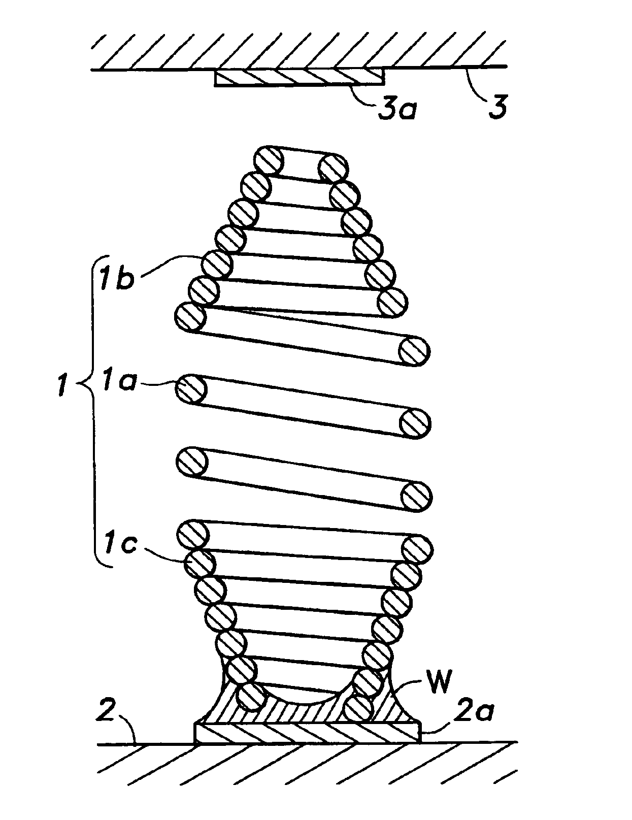
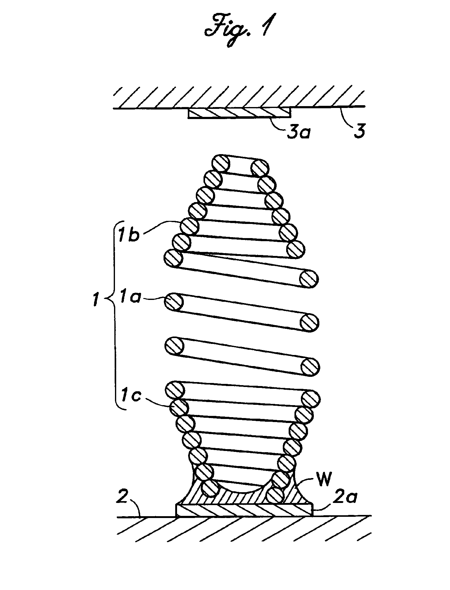
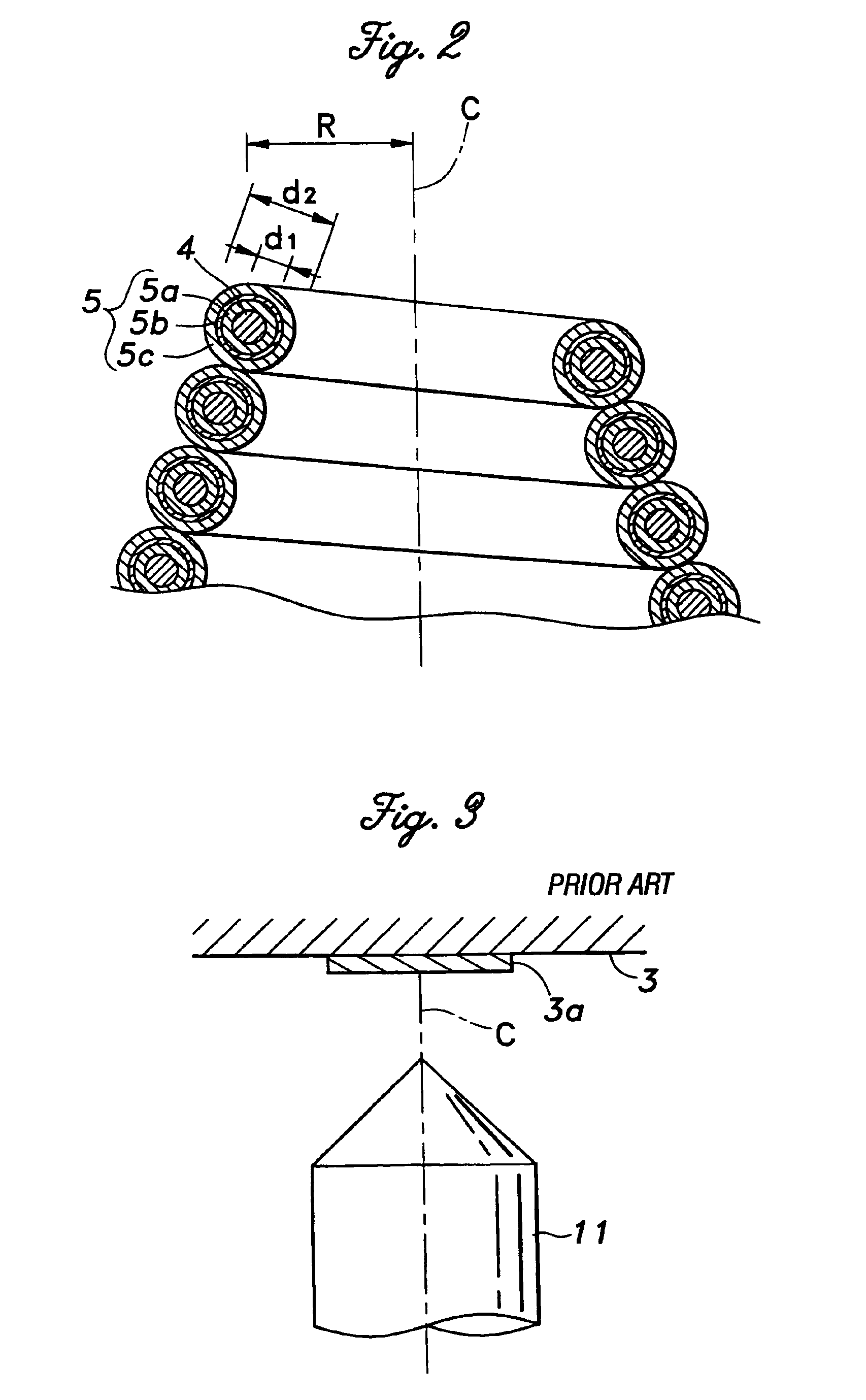
Thus, the core wire is coiled to a smallest possible radius in the last turn, and the coil wire diameter is thereafter increased by forming layers formed by plating or other similar methods. The final result is that the last turn of the coil wire at the free end has a smaller coil radius than would be possible by coiling the coil wire. The reduction in the coil radius of the last turn contributes to the improvement in the positional accuracy of the free end of the tapered end of the conductive coil contact member.
The soldering connection for the second tapered end ensures both the positional stability and favorable electric property of the conductive coil contact member. Because of the conical shape of the second tapered end, it is possible to ensure a stable connection even if the amount of applied solder is small owing to the small cross sectional area of the free end of the second tapered end, and prevent the solder from reaching the compression coil spring portion and impairing the spring function thereof owing to the capability of the second tapered end to retain a pool of solder inside the tapered turns of the coil wire.

Problems solved by technology

A conductive coil contact member allows the electric inductance and resistance to be minimized, but causes some difficulty in achieving the positional accuracy of its tip with respect to the object to be contacted.
Such an offset can be reduced by reducing the radius of the last turn, but it is difficult to reduce the radius of a turn beyond a certain limit for a given diameter of the coil wire.
If a coil wire having a small diameter is used, it is possible to reduce the radius of the turn, but the desired resiliency or rigidity of the contact member may not be achieved, and the electric inductance and resistance inevitably increase.
Such an arrangement permits the positional accuracy of each tip to be increased without any limit in theory, but becomes impractical when the size of the conductive coil contact member is reduced beyond a certain level.

Method used


Image

  • Conductive coil contact member
  • Conductive coil contact member
  • Conductive coil contact member

Examples


second embodiment

FIG. 9 shows the present invention in which the parts corresponding to those of the previous embodiment are denoted with like numerals. In this embodiment, the through hole 9 of the insulating plate member 7 facing away from the circuit board 2 is not different from that of the previous embodiment, but the through hole 11 formed in the lower insulating plate 8 on the side of the circuit board 2 consists of a small diameter portion 11a similar to that shown in FIG. 7 and a large diameter portion 11b provided on the side of the circuit board 2. The large diameter portion 11b is so dimensioned as to expose the circuit terminal 2a even when the lateral relative positioning between the holder and the circuit board 2 is not perfect. The large diameter portion 11a consists of a straight hole, and this simplifies the work of forming the hole.

third embodiment

FIG. 10 shows the present invention in which the parts corresponding to those of the previous embodiments are denoted with like numerals. In this embodiment, the through hole 9 of the insulating plate member 7 facing away from the circuit board 2 is not different from that of the previous embodiment, but the through hole 12 formed in the lower insulating plate 8 on the side of the circuit board 2 consists of a straight small diameter hole extending over the entire thickness of the insulating plate 8. This simplifies the work of forming the hole, and contributes to the reduction of the manufacturing cost.

fourth embodiment

FIG. 11 shows the present invention in which the parts corresponding to those of the previous embodiments are denoted with like numerals. In this embodiment, the holder in this case consists of a single insulating plate member 13 which is connected to the circuit board 2. A through hole 14 passed across the thickness of the insulating plate member 13 comprises a large diameter portion 1c extending from the end adjoining the circuit board 2 over a large part of the thickness of the insulating plate member 13, a small diameter portion 14b extending over a short distance from the end facing away from the circuit board 2, and a tapered portion 14c which smoothly connects the large diameter portion 14a and small diameter portion 14b together.

According to this embodiment, the holder for retaining the conductive coil contact member 1 can be simplified. Similarly as the embodiment illustrated in FIG. 7, the conical electrode portion 1b resiliently abuts the tapered portion 14c of the throug...


PUM


Abstract

In a conductive coil contact member having at least one tapered end consisting of a plurality of turns of coil wire having a progressively smaller coil radius toward a free end thereof, the coil wire comprises a core wire and at least one highly electrically conductive layer formed over the core wire, a last turn of the coil wire at the free end having a smaller coil radius than would be possible by coiling the coil wire. Thus, the core wire is coiled to a smallest possible radius in the last turn, and the coil wire diameter is thereafter increased by forming layers formed by plating or other similar methods. The final result is that the last turn of the coil wire at the free end has a smaller coil radius than would be possible by coiling the coil wire. The reduction in the coil radius of the last turn contributes to the improvement in the positional accuracy of the free end of the tapered end of the conductive coil contact member.

Description

TECHNICAL FIELDThe present invention relates to a conductive coil contact member suitable for use in contact probes and contact cards for testing semiconductor devices and wafers, electric sockets for devices in such forms as LGA (land grid array), BGA (ball grid array), CSP (chip side package) and bare chip, and electric connectors. The present invention also relates to a contact probe head using a conductive coil contact member.BACKGROUND OF THE INVENTIONConventionally, various forms of conductive contact members have been used in electrically testing (open / short circuit tests, environmental tests, burn-in tests and so forth) electroconductive patterns of printed circuit boards and electronic components, and have been widely used in contact probes for testing wafers, electric sockets for semiconductor devices in such forms as LGA, BGA, CSP and bare chip, and connectors.In applications to electric sockets for semiconductor devices, for instance, there is a trend for using higher si...

Claims


Application Information

Patent Timeline
Patent Type & Authority Patents(United States)
IPC IPC(8): G01R1/067
CPCG01R1/06716G01R1/0483G01R1/0466
Inventor KAZAMA, TOSHIO
Owner NHK SPRING CO LTD
Learn More