

Adaptive MOSFET resistor
- Summary
- Abstract
- Description
- Claims
- Application Information
AI Technical Summary
Benefits of technology
Problems solved by technology
Method used
Image

Examples
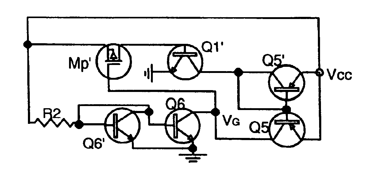
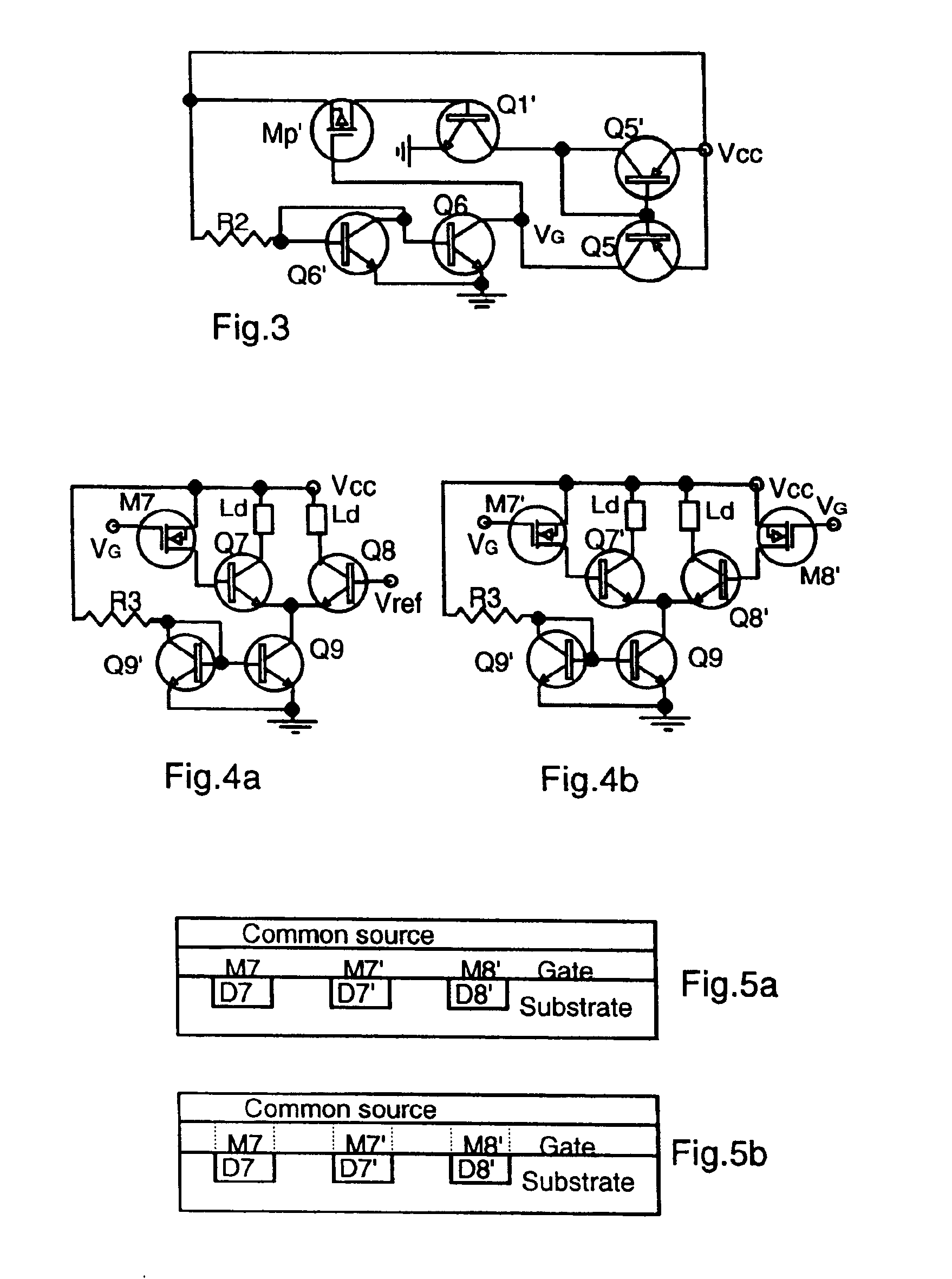
Embodiment Construction
Operation of the MOSFET Resistor:
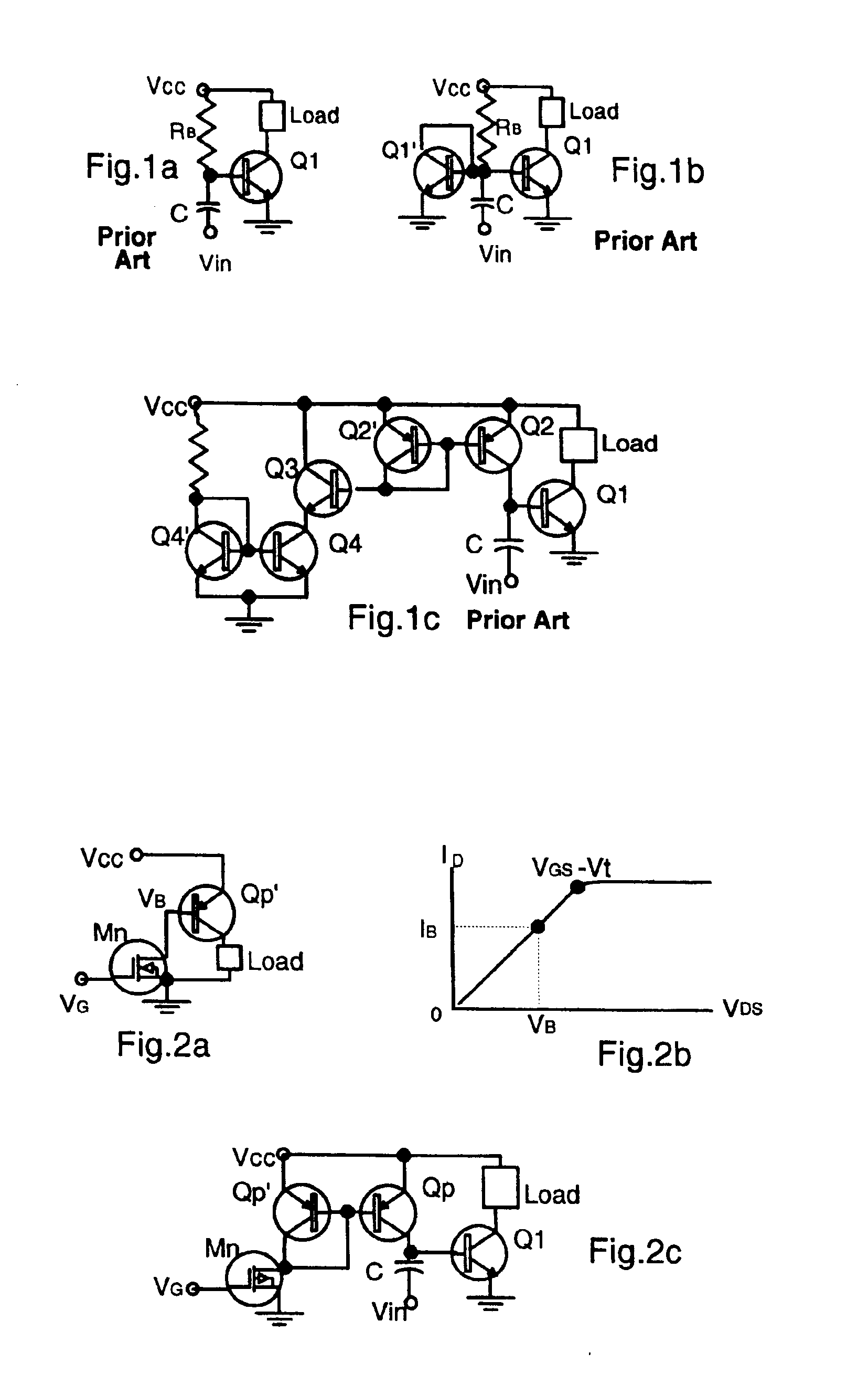
FIG. 2a shows the use of a n-channel MOSFET Mn as a base resistor for biasing a pnp BJT Qp of a common emitter amplifier. The dc drain characteristic is shown in FIG. 2b. The current ID of a MOSFET is given as:
ID=kp(W / L)[(VGS−Vt) VDS−VDS2 / 2] (1)
where kp is a transconductance parameter, W / L is the width-to-length ratio of the gate, VGS is the gate to source voltage, Vt is the threshold voltage and VDS is drain-to-source voltage. When VDS is less than (VGS−Vt), the MOSFET is operating in the ohmic region, and
IC≈kp(W / L)(VGS−Vt) VDS (2)
The ohmic resistance is:
RDS=VDS / IC=1 / [kp(VGS−Vt)] (3)
By adjusting VGS, a wide range of resistance values can be obtained, so long as VDS is less than (VGS−Vt).
FIG. 2c shows the use of Qp′ similar to the pnp amplifier shown in FIG. 2a as the master section of a current mirror fed from the MOSFET resistor Mn. The slave section Qp mirrors the current through Mn to the master section Qp′. The gate voltage VG is adjusted ...
PUM
 Abstract
Description
Claims
Application Information