Printed circuit board noise attenuation using lossy conductors

a technology of lossy conductors and printed circuit boards, which is applied in cross-talk/noise/interference reduction, line-transmission details, waveguide type devices, etc., can solve problems such as affecting the normal operation of circuitry, inducing electric current or electromagnetic interference (emi), and increasing switching noise at higher frequencies. , to achieve the effect of attenuating noise and attenuating nois

Inactive Publication Date: 2005-03-29
HEWLETT PACKARD DEV CO LP
View PDF5 Cites 25 Cited by
  • Summary
  • Abstract
  • Description
  • Claims
  • Application Information

AI Technical Summary

Problems solved by technology

Consequently, the electromagnetic fields emitted by one electric device may induce electric current, or electromagnetic interference (EMI), in a different electric device.
If the amplitude of the EMI is high enough, it may disrupt normal operations of circuitry.
Switching rates and switching current amplitudes are increasing with each new generation of chip design, contributing to increased switching noise at higher frequencies.
Noise on the power and ground planes, and particularly switching noise on power planes, may interfere with operation of the integrated circuits connected to the printed circuit board.
If power and ground plane noise is too great, it may cause interference in an integrated circuit that result in faulty operation of an electronic device.
These types of errors may be intermittent, and therefore, very difficult to diagnose.
These intermittent failures may happen more frequently than users or designers realize.
Existing techniques for noise reduction, including the use of multiple low-inductance bypass capacitors, are becoming increasingly less effective at the higher frequencies used by newer integrated circuits.
Bypass capacitors of either the low-pass or the high-pass type intrude on valuable board space, making the board larger, and generally more expensive, than it otherwise would need to be.
The I2R loss in the conductors of the current-carrying planes attenuates the higher frequency noise.
As transistor densities increase within integrated circuits, the associated EMI and noise restrictions become increasingly difficult to meet.
Large copper planes, however, and ground planes in particular, are very difficult to filter effectively, making power and ground planes significant contributors to EMI and noise.

Method used


Image

  • Printed circuit board noise attenuation using lossy conductors
  • Printed circuit board noise attenuation using lossy conductors
  • Printed circuit board noise attenuation using lossy conductors

Examples


Embodiment Construction

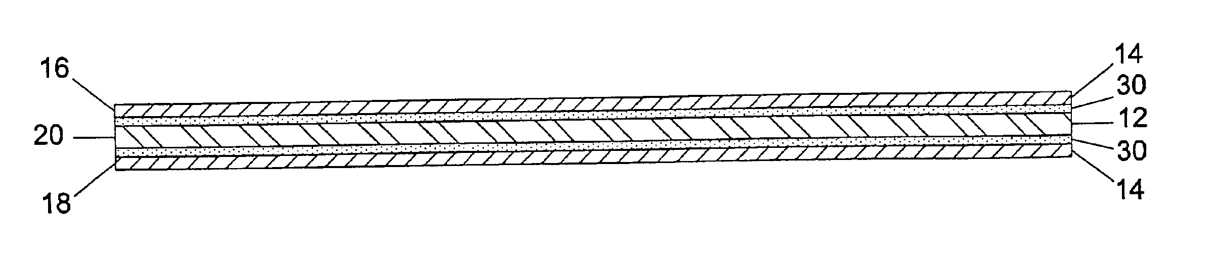
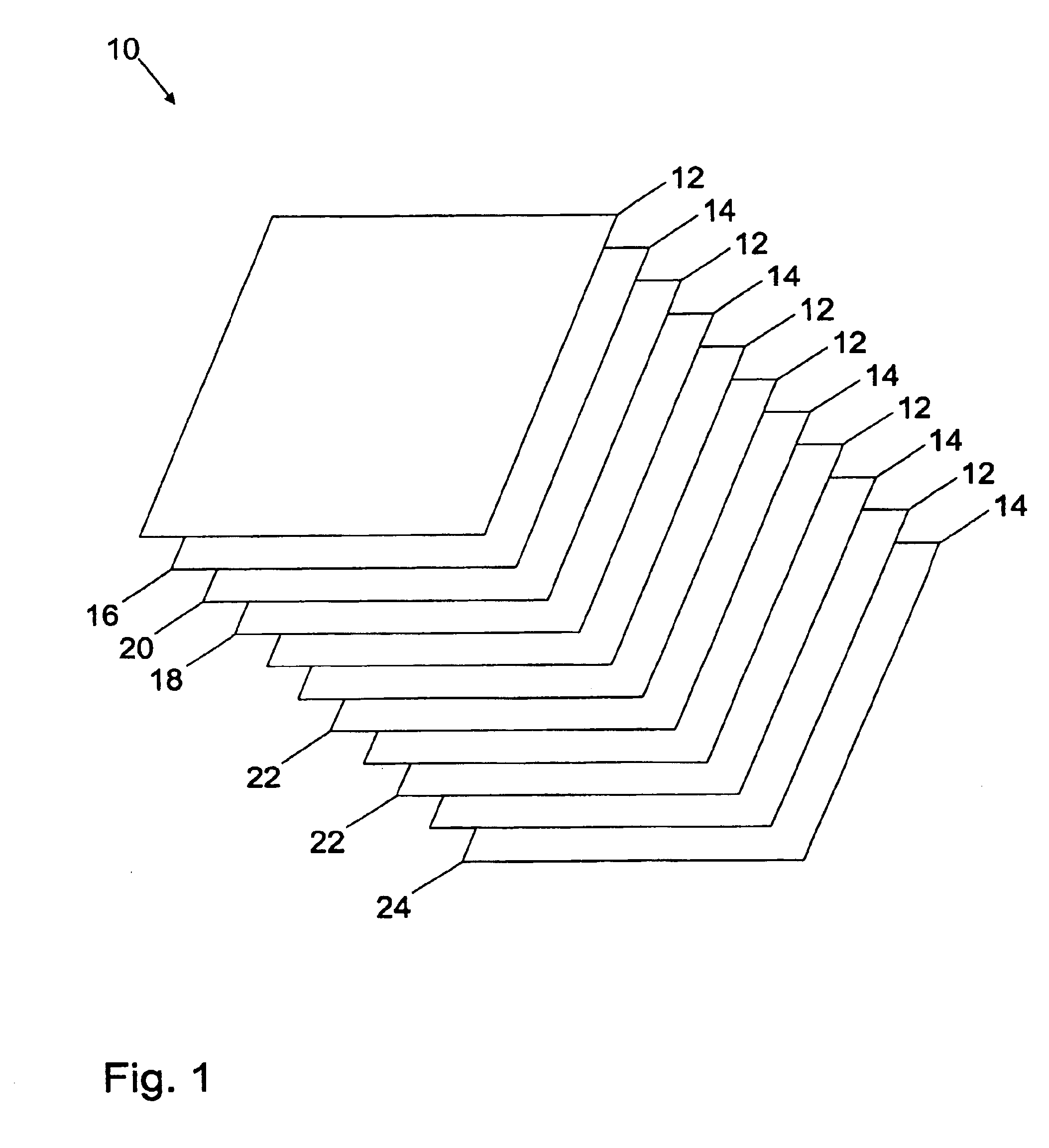
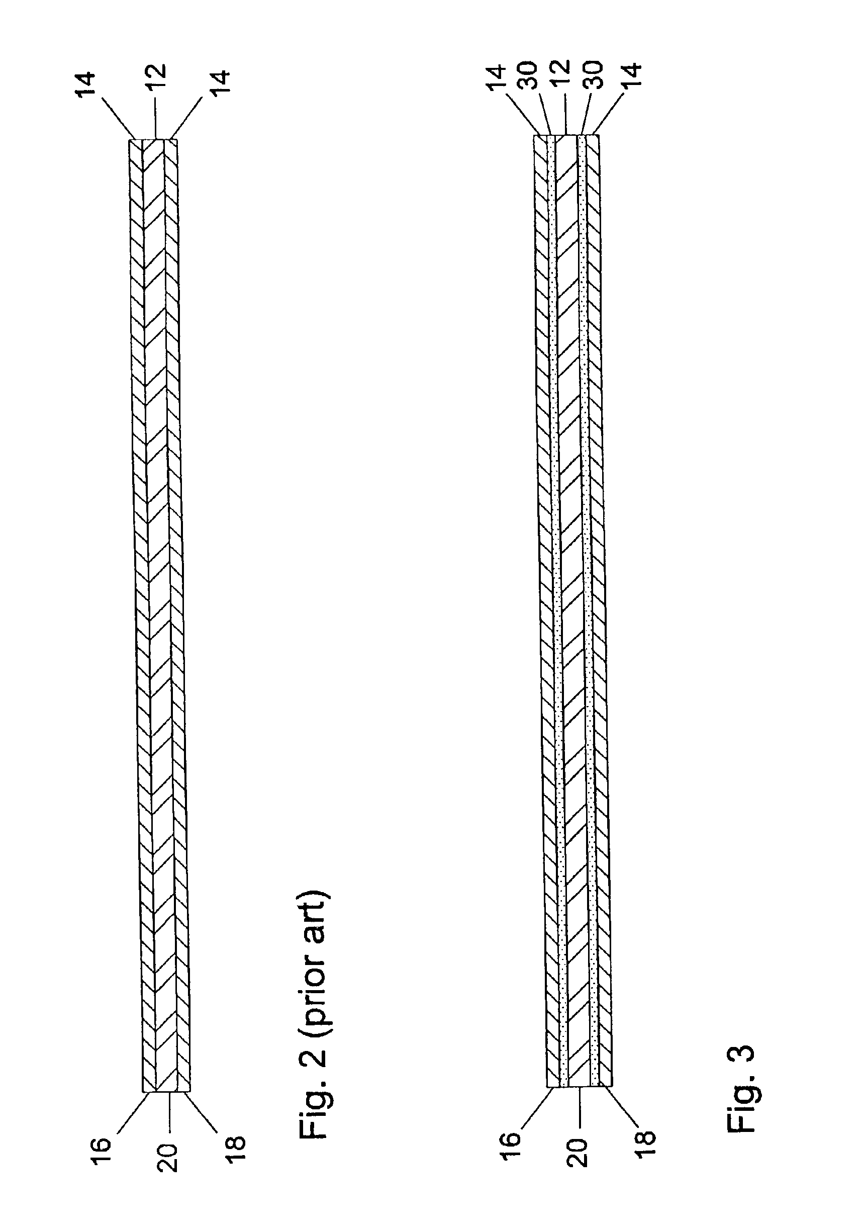
In accordance with the present invention, a method and related device are disclosed for isolating paired power and ground plane layers from dielectric (or electrically insulating) layers within a printed circuit board (PCB) with thin, lossy laminates, or layers of material relatively low in conductivity when compared to adjacent conductive layers. Referring now to FIG. 1, the present invention may be better understood by understanding a few key aspects of printed circuit boards. To form a printed circuit board 10, insulating layers 12 and conductive layers 14 are laminated together, generally with one or more insulating layers 12 separating each conductive layer 14. Insulating layers 12 are generally made of a ceramic, such as alumina, or other dielectric material, such as FR-4, a glass epoxy resin commonly used in printed circuit board fabrication. Conductive layers 14 are generally made of a metal with a high electrical conductivity, such as copper (Cu) or tungsten (W). One of the...


PUM


Abstract

A method and related configuration for attenuating high-frequency noise that may appear on power planes in printed circuit boards. In one embodiment, the noise attenuation means of the present invention involves applying a lower conductivity material between the conductive and dielectric layers within a printed circuit board. High-frequency noise is then attenuated by the skin effect. In another embodiment, the low conductivity material is applied between the power plane and dielectric layer within the printed circuit board. The low conductivity material may be a material, such as nickel or lead, having an electrical conductivity ranging between about 1×10⁴ mhos / m and 5.8×10⁷ mhos / m for layers having a thickness of about 2 mils.

Description

BACKGROUNDA wide variety of electrical devices have become part of everyday life. In a typical day, a person may use an alarm clock, a computer, a television, and countless other electrically powered tools and appliances. The electric current used to operate each of these devices produces both electric fields and magnetic fields, collectively referred to herein as electromagnetic fields. As current passes through a conductive material, the conductor acts like an antenna, transmitting electromagnetic fields into the surrounding environment much like a radio transmission antenna. Conversely, when a conductor is placed in an electromagnetic field, current is induced in the conductor, much like a radio reception antenna. Consequently, the electromagnetic fields emitted by one electric device may induce electric current, or electromagnetic interference (EMI), in a different electric device. Also, depending on the frequency of the emissions, EMI is sometimes also referred to as radio freq...

Claims


Application Information

Patent Timeline
Patent Type & Authority Patents(United States)
IPC IPC(8): H05K1/16H05K1/02
CPCH05K1/0234H05K1/167H05K2203/0723H05K2201/09309H05K2201/0355
Inventor GREBENKEMPER, JOHN
Owner HEWLETT PACKARD DEV CO LP
Why Eureka
Try Eureka