Non-abrupt switching of sleep transistor of power gate structure

a technology of power gate structure and sleep transistor, which is applied in the direction of electronic switching, pulse technique, instruments, etc., can solve the problems of serious circuit performance degradation, primary source of power consumption of cmos design, and critical design concern, so as to reduce ground bounce, reduce voltage glitches the effect of magnitude and minimum tim

Inactive Publication Date: 2005-04-05
MEDIATEK INC
View PDF4 Cites 37 Cited by
  • Summary
  • Abstract
  • Description
  • Claims
  • Application Information

AI Technical Summary

Benefits of technology

A semiconductor integrated circuit including a non-abrupt switching mechanism for a sleep transistor of a power gate structure to reduce ground bounce is described. The switching mechanism reduces the magnitude of voltage glitches on the power and ground rails as well as the minimum time required to stabilize power and ground.

Problems solved by technology

As the number of devices being packed into a system-on-a-chip (SoC) approaches millions, power consumption has become a critical design concern due to the increasing gap between the energy required by portable computation / communication devices and the energy supplied by the battery.
Traditionally, the primary source of power consumption for a CMOS design comes from the switching of logic states.
Reducing Vdd alone, however, causes serious circuit performance degradation.
Reducing Vth, however, exponentially increases subthreshold leakage current.
This problem escalates in deep-submicron (DSM) technologies.
In DSM technologies, the supply voltage is scaled down aggressively, causing the resistance of the sleep transistor to increase dramatically, requiring larger size sleep device.
If the magnitude of this voltage surge / drop is greater than the noise margin of a circuit, the circuit may erroneously latch the wrong value or switch at the wrong time.
In designs employing a power gate structure to control leakage power, however, ground bounce due to switching of the sleep transistor is a potential problem.

Method used


Image

  • Non-abrupt switching of sleep transistor of power gate structure
  • Non-abrupt switching of sleep transistor of power gate structure
  • Non-abrupt switching of sleep transistor of power gate structure

Examples


second embodiment

FIG. 7 is a schematic diagram of a power gate structure including a non-abrupt switching mechanism according to the present invention.

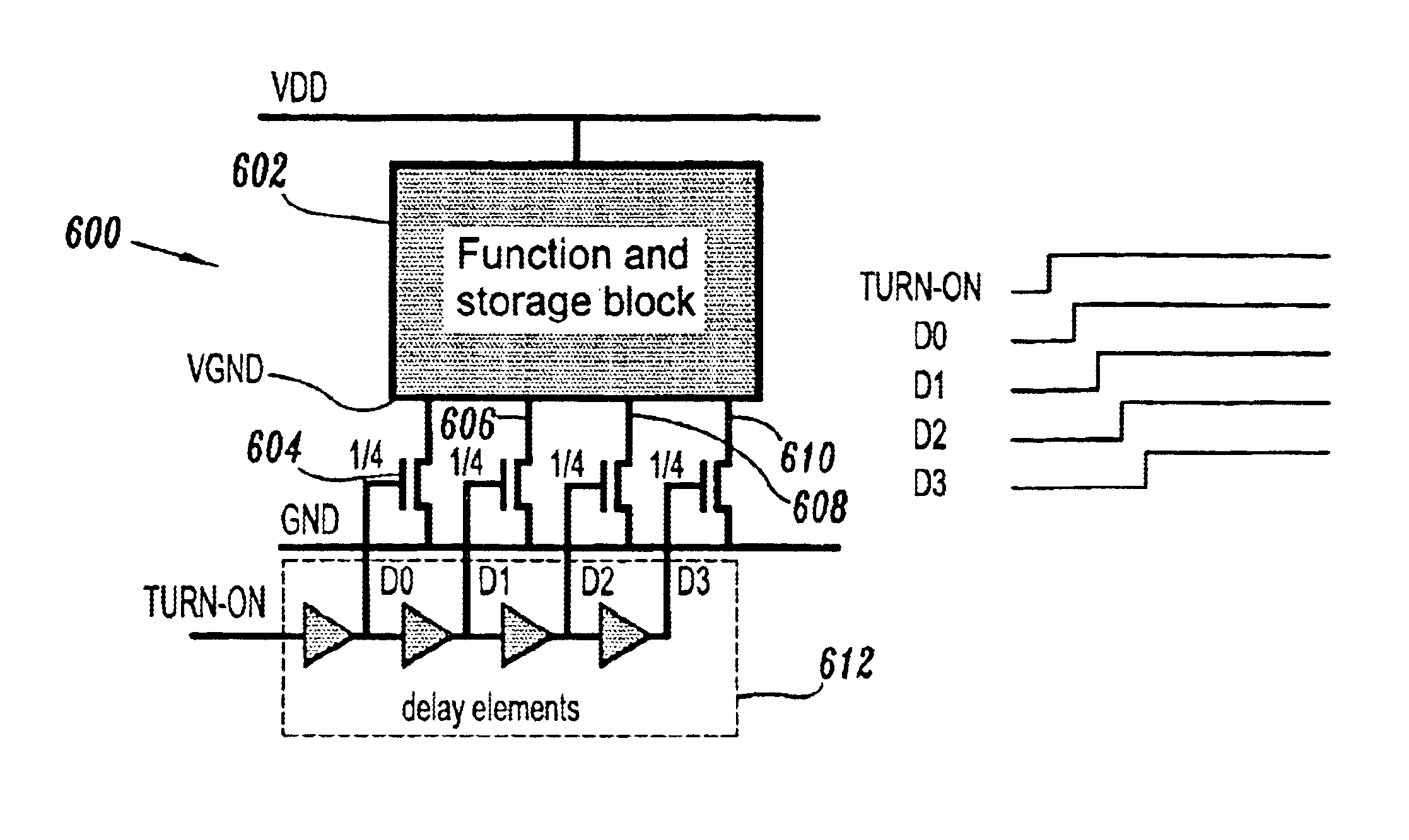
The power gate structure 700 of FIG. 7 includes a supply voltage line VDD, a ground voltage line GND, a virtual ground voltage line VGND, a logic circuit 702 coupled to the supply voltage line VDD and the virtual ground voltage line VGND, a plurality of sleep transistors 704-710 for controlling current flow to the logic circuit 702, the sleep transistors 704-710 being coupled to the virtual ground voltage line VGND and the ground voltage line GND; and a stepwise switching circuit 712 for sequentially controlling the sleep transistors 704-710. The logic circuit 702 may contain any number of logic elements for performing a function of a semiconductor device or for storing data.

The switching circuit 712 is a shift register including a plurality of outputs Q0-Q3. Each output Q0-Q3 corresponds to a single sleep transistor 704-710. As the semiconductor devi...

third embodiment

FIG. 8 is a schematic diagram of a power gate structure including a non-abrupt switching mechanism according to the present invention.

The power gate of structure 800 of FIG. 8 includes a supply voltage line VDD, a ground voltage line GND, a virtual ground voltage line VGND, a logic circuit 802 coupled to the supply voltage line VDD and the virtual ground line VGND, a series of sleep transistors 804 and 805 for controlling the current flow to the logic circuit of 802, the sleep transistors 804 and 805 being coupled to the virtual ground voltage line VGND and the ground voltage line GND, a discharge capacitor 806 connected to an intermediate node N1 between sleep transistors 804 and 805 and the ground voltage line GND; and a pulse generator circuit 812 for sequentially controlling sleep transistors 804 and 805 to incrementally transfer charge from the virtual ground line VGND to the discharge capacitor 806 via the transistor 804, then from the discharge capacitor 806 to the ground lin...


PUM


Abstract

A semiconductor integrated circuit including a non-abrupt switching mechanism for a sleep transistor of a power gate structure to reduce ground bounce is provided. The semiconductor integrated circuit comprises a supply voltage line; a ground voltage line; a virtual ground voltage line; a logic circuit coupled to the supply voltage line and the virtual ground voltage line; at least one sleep transistor for controlling current flow to the logic circuit, the sleep transistor being coupled to the virtual ground voltage line and the ground voltage line; and a non-abrupt switching circuit for sequentially controlling the sleep transistor. The switching mechanism reduces the magnitude of voltage glitches on the power and ground rails as well as the minimum time required to stabilize power and ground.

Description

BACKGROUND OF THE INVENTION1. Field of the InventionThe present invention relates generally to semiconductor integrated circuit design, and more particularly, to a non-abrupt switching mechanism for a sleep transistor of a power gate structure for reducing ground bounce.2. Description of the Related ArtAs the number of devices being packed into a system-on-a-chip (SoC) approaches millions, power consumption has become a critical design concern due to the increasing gap between the energy required by portable computation / communication devices and the energy supplied by the battery. Traditionally, the primary source of power consumption for a CMOS design comes from the switching of logic states. The switching power is expressed asPswitch=a0→1·f·clk(Cload·V2dd) where 0→1 is the average number of times in a clock cycle that a switch from 0 to 1 occurs, fclk is the clock frequency, Cload is the load capacitance and Vdd is the supply voltage.The equation clearly shows that supply voltage ...

Claims


Application Information

Patent Timeline
Patent Type & Authority Patents(United States)
IPC IPC(8): H03K17/16
CPCH03K17/164H03K17/163
Inventor KIM, SUHWANKNEBEL, DANIEL R.KOSONOCKY, STEPHEN V.
Owner MEDIATEK INC
Why Eureka
Try Eureka