System and method for generating a mask layout file to reduce power supply voltage fluctuations in an integrated circuit

a technology of power supply voltage and layout file, applied in the field of semiconductor design, can solve the problems of false switching of logic gates, additional signal delay, ringing in the output waveform or delay in response speed, etc., and achieve the effect of substantially reducing power supply voltage fluctuations in the integrated circui

a technology of power supply voltage and layout file, applied in the field of semiconductor design, can solve the problems of false switching of logic gates, additional signal delay, ringing in the output waveform or delay in response speed, etc., and achieve the effect of substantially reducing power supply voltage fluctuations in the integrated circui

US6877144B1Inactive Publication Date: 2005-04-05CELERICS TECH

Image

  • System and method for generating a mask layout file to reduce power supply voltage fluctuations in an integrated circuit
  • System and method for generating a mask layout file to reduce power supply voltage fluctuations in an integrated circuit
  • System and method for generating a mask layout file to reduce power supply voltage fluctuations in an integrated circuit

Examples


Embodiment Construction

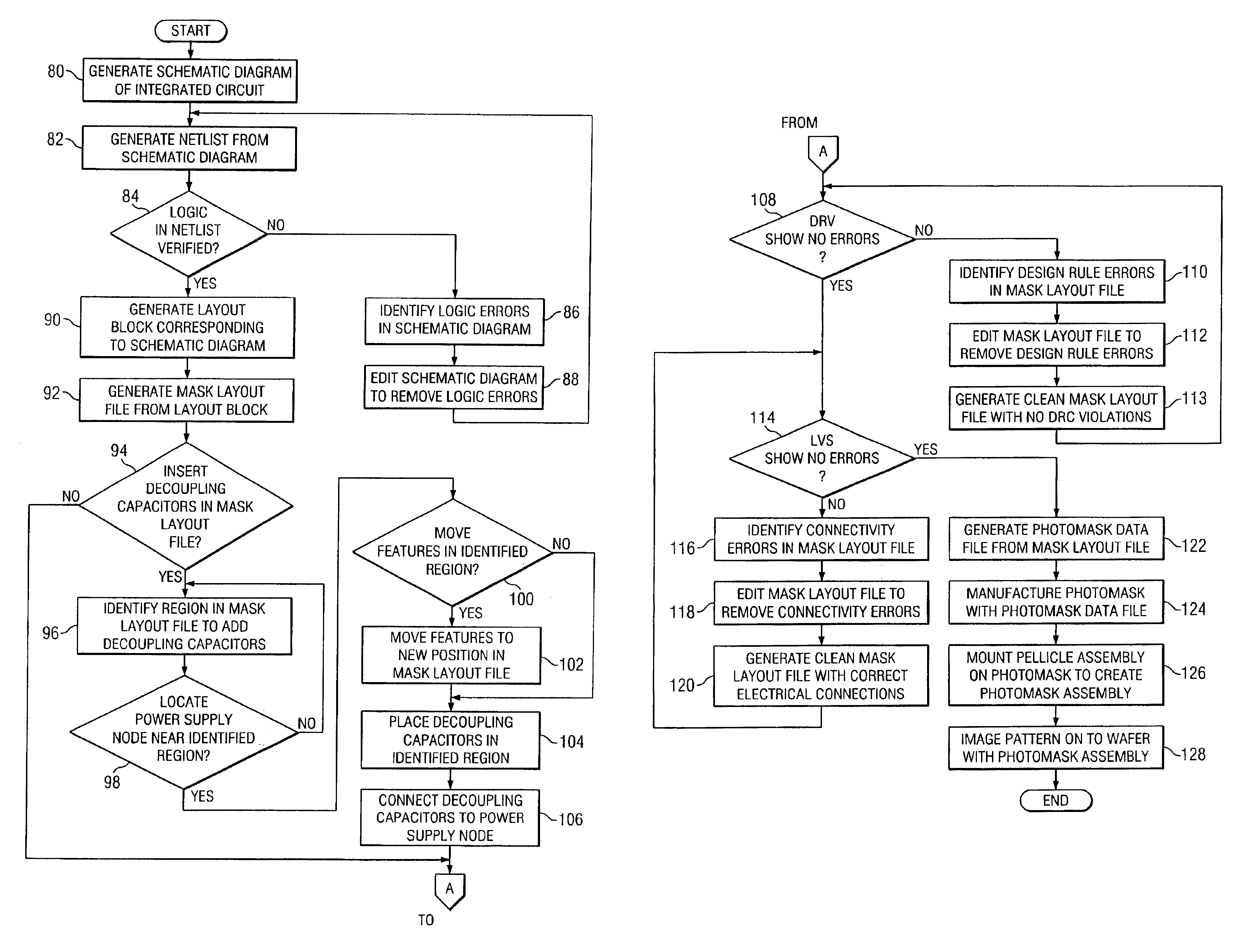
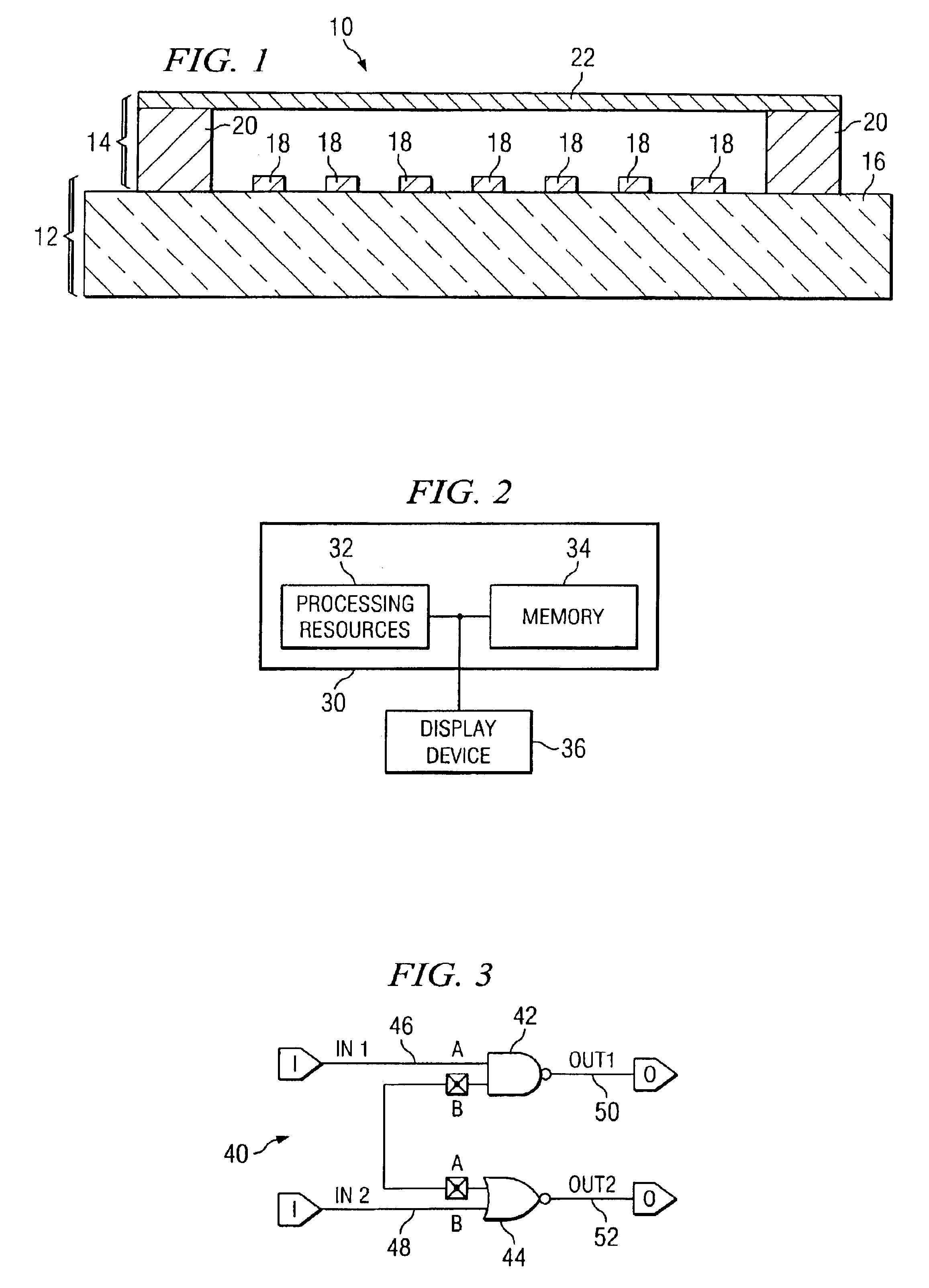
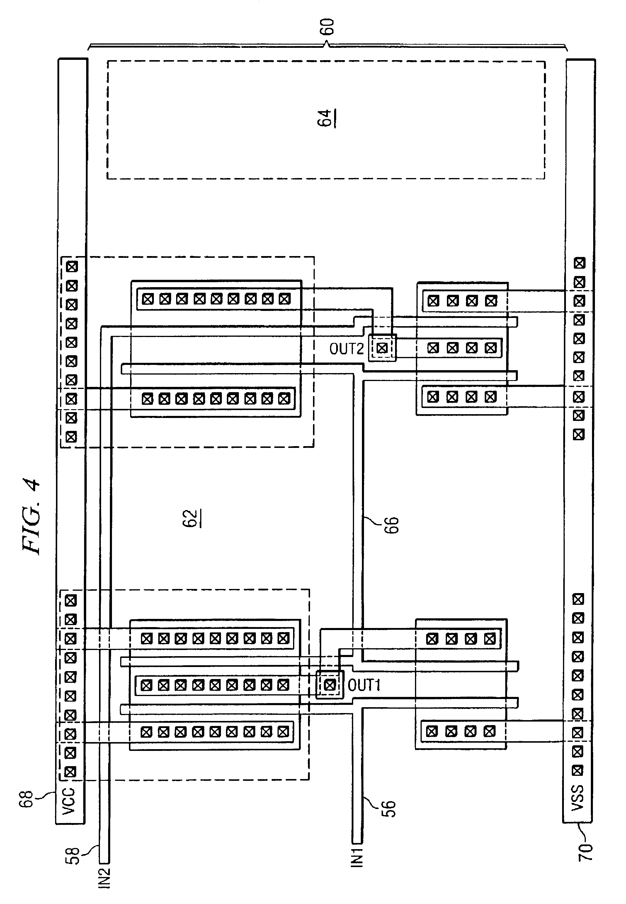
Preferred embodiments of the present invention and their advantages are best understood by reference to FIGS. 1 through 6, where like numbers are used to indicate like and corresponding parts.

As the number of transistors on an integrated circuit (IC) continues to increase, the design process for the IC becomes more complex. For example, an increasing number of transistors may require additional layers to form the IC on a semiconductor wafer. Each layer associated with the IC may include one or more design rules for the individual layer in a desired manufacturing process. The number of design rules for the desired manufacturing process, therefore, increases with the number of layers formed on the semiconductor wafer.

A design rule typically defines the minimum or maximum allowable dimension for a feature fabricated on a specific layer. For example, an IC may include, among other layers, a diffusion layer that forms a decoupling capacitor and / or the source and drain regions of a transi...


PUM


Abstract

A system and method for generating a mask layout file to reduce power supply voltage fluctuations in an integrated circuit are disclosed. The method includes analyzing a pattern in a mask layout file to identify a region in the pattern to add one or more decoupling capacitors. Once the region is identified, a feature located in the identified region is moved based on a design rule from a first position to a second position in the mask layout file to create a space in the identified region. The decoupling capacitors are automatically placed in the space in the identified region.

Description

TECHNICAL FIELD OF THE INVENTIONThis invention relates in general to the field of semiconductor design, and more particularly to a system and method for generating a mask layout file to reduce power supply voltage fluctuations in an integrated circuit.BACKGROUND OF THE INVENTIONA typical semiconductor design process includes numerous steps. Initially, a circuit designer prepares a schematic diagram that includes logical connections between logic elements that form an integrated circuit. The schematic diagram is then tested to verify that the logic elements and associated logical connections perform a desired function. Once the circuit is verified, the schematic diagram is converted into a mask layout database that includes a pattern of polygons. The polygons may represent the logic elements and the logical connections contained the schematic diagram. The mask layout database is then converted into multiple photomasks, also know as masks or reticles, that may be used to image differe...

Claims


Application Information

Patent Timeline
05 Apr 2005
Publication
US6877144B1
IPC
G06F17/50
CPC
G06F17/5068; G06F30/39
Inventors
RITTMAN, DANNY; OREN, MICHA