System and method for compensating for supply voltage induced clock delay mismatches

a supply voltage and clock delay technology, applied in the field of electronic circuits, can solve the problems of consuming more power than a comparable circuit, and requiring a trade-off between the speed at which a circuit operates and the power it consumes, so as to reduce the delay mismatch

Inactive Publication Date: 2005-04-12
AVAGO TECH INT SALES PTE LTD
View PDF6 Cites 12 Cited by
  • Summary
  • Abstract
  • Description
  • Claims
  • Application Information

AI Technical Summary

Benefits of technology

One embodiment of a system constructed according to the invention incorporates a buffer with an adjustable delay to reduce the delay mismatch between clock signals driven by clock trees associated with each operating voltage. A phase detector circuit compares the clock phases for rising and falling edges of the clock signals for each operating voltage. The phase detector circuit controls bias voltages that, in turn, control the delay of the adjustable-delay buffer.

Problems solved by technology

However, tradeoffs typically must be made between the speed at which a circuit operates and the power the circuit consumes.
In general, a circuit that operates at a higher speed than a comparable circuit will consume more power than that comparable circuit.
In many circumstances, there is a practical limit on the amount of power a given circuit can or should consume.
For example, increased power consumption typically results in a higher overall cost for the system.
Moreover, certain types of electronic circuits such as integrated circuits can only dissipate a limited amount of power.
High power consumption may also have other adverse effects on the operation of a circuit such as reducing the reliability of the circuit and adversely affecting the timing relationships in the circuit.
As in virtually all electronic circuits, the circuit components that generate the clock signals induce a delay in signals that pass through them.
As a result of these delays, the clocks that drive the circuit components that operate at different supply voltages may be skewed in time relative to one another.
Moreover, this skew in time may vary over time as the supply voltages deviate within their operating tolerances.
This misalignment of the clock signals in the different domains may result in clock uncertainty.
This, in turn, may reduce the available cycle time of the circuit because the clock uncertainty has to be compensated by asynchronous delays when a signal is exchanged between the two domains within one clock cycle.
As a result, it may be impossible to double latch the signals.
In sum, this misalignment of the clock signals may corrupt data being processed by the circuit.

Method used


Image

  • System and method for compensating for supply voltage induced clock delay mismatches
  • System and method for compensating for supply voltage induced clock delay mismatches
  • System and method for compensating for supply voltage induced clock delay mismatches

Examples


Embodiment Construction

The invention is described below, with reference to detailed illustrative embodiments. It will be apparent that the invention can be embodied in a wide variety of forms, some of which may be quite different from those of the disclosed embodiments. Consequently, the specific structural and functional details disclosed herein are merely representative and do not limit the scope of the invention.

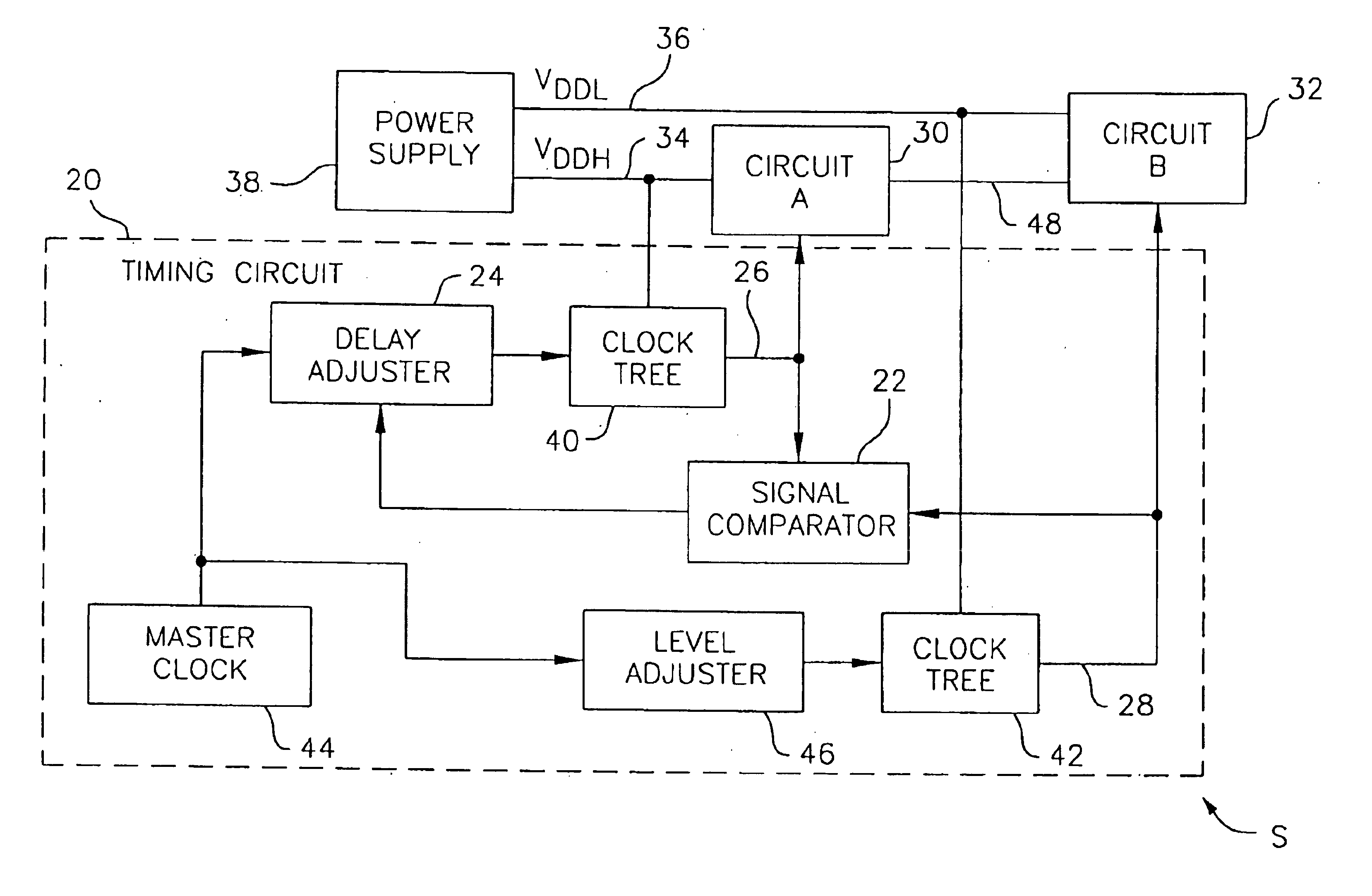
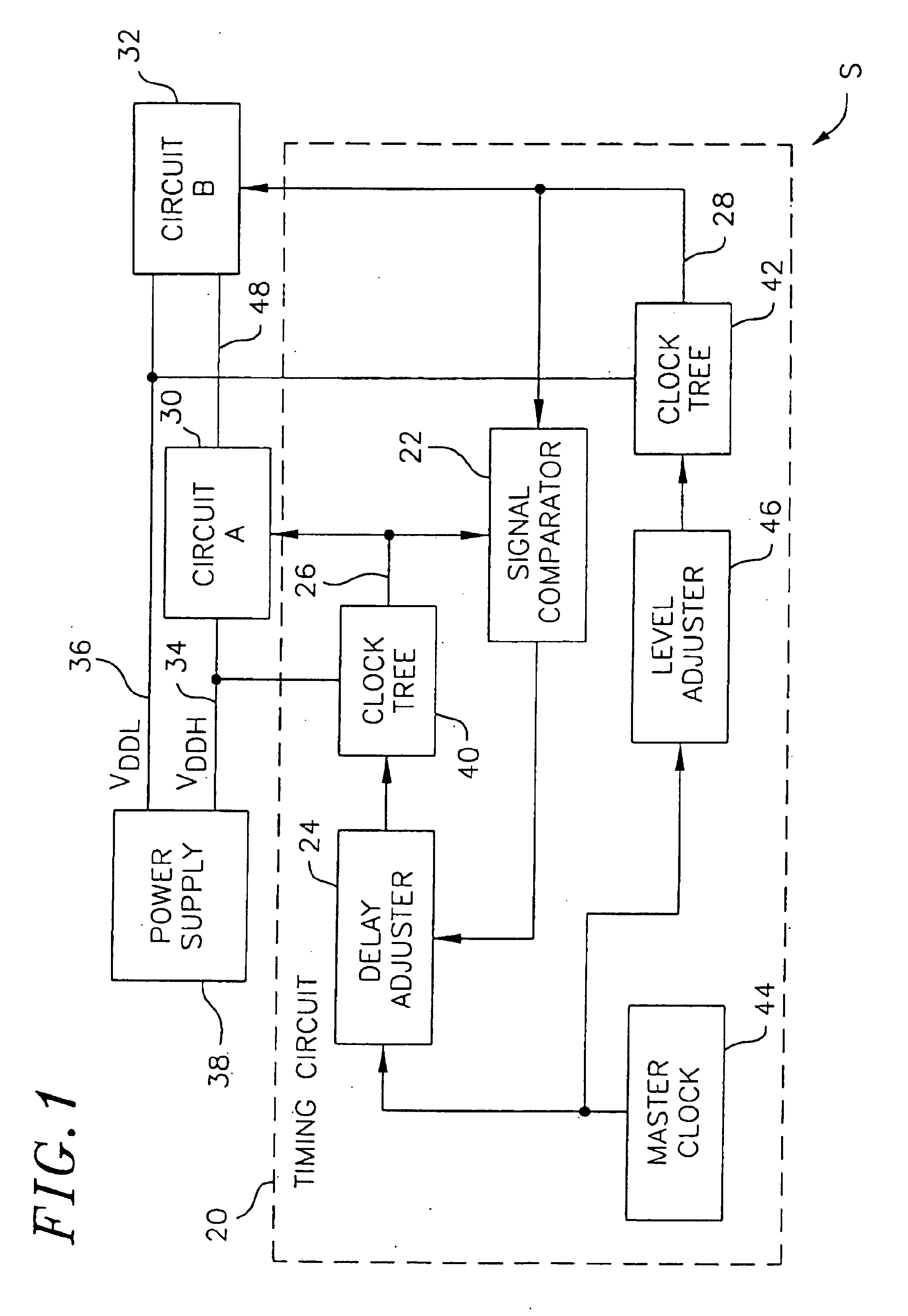
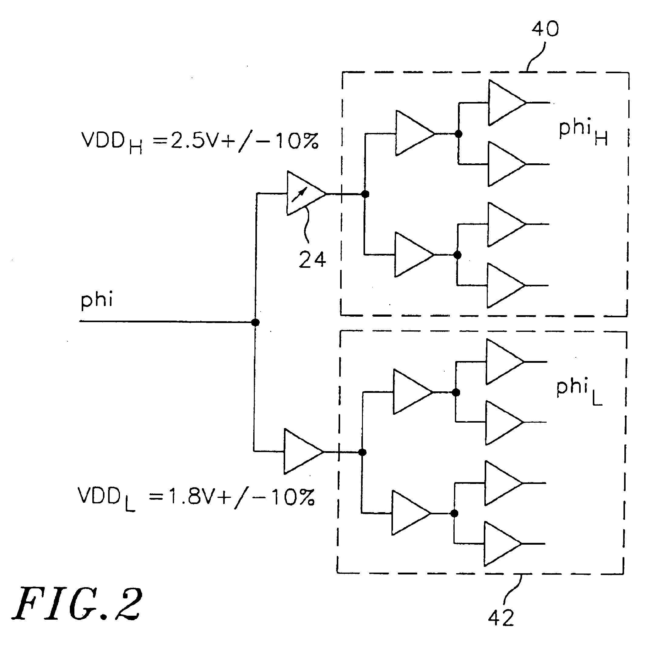
FIG. 1 is a block diagram of one embodiment of a system utilizing clock delay compensation in accordance with the present invention. Specifically, the system S incorporates a timing circuit 20 that includes a signal comparator 22 and a delay adjust circuit 24 for maintaining phase synchronization between clocks 26 and 28 that drive circuit A 30 and circuit B 32, respectively.

The system of FIG. 1 typically is implemented in an integrated circuit where multiple supply voltages are used to reduce the power dissipation of the integrated circuit. In this case, less timing-critical parts operate on a...


PUM


Abstract

Various systems and methods providing signal delay compensation for circuits such as a multi-pair gigabit Ethernet transceiver are disclosed. In an analog implementation a buffer with an adjustable delay may be used to minimize the delay mismatch between clock trees. The delay of the adjustable-delay buffer is controlled by bias voltages that determine the charging and discharging current to the adjustable buffer. A phase detector circuit is used to compare the clock phases for rising and falling edges, and to adjust the bias voltages that control these edges. In a digital implementation a selector switch, responsive to a phase detector, may be used to route clock signals through circuit elements to delay clock signals.

Description

FIELD OF THE INVENTIONThe present invention relates generally to electronic circuits and, more particularly, to efficient clock domain partitioning and clock delay matching.BACKGROUND OF THE INVENTIONThere is a perpetual need for increased operating speed in electronics circuits used in electronic equipment. For example, circuit designers are continually developing communication circuits and microprocessors that can send and process data, respectively, at faster and faster rates.However, tradeoffs typically must be made between the speed at which a circuit operates and the power the circuit consumes. In general, a circuit that operates at a higher speed than a comparable circuit will consume more power than that comparable circuit. In many circumstances, there is a practical limit on the amount of power a given circuit can or should consume. For example, increased power consumption typically results in a higher overall cost for the system. Moreover, certain types of electronic circu...

Claims


Application Information

Patent Timeline
Patent Type & Authority Patents(United States)
IPC IPC(8): G06F1/10G06F3/00H03L7/087H03L7/081H03L7/08
CPCG06F1/10G06F3/002H03L7/087H03L7/0814H03L7/081
Inventor LUTKEMEYER, CHRISTIAN A.J.
Owner AVAGO TECH INT SALES PTE LTD
Why Eureka
Try Eureka