

Spherical lens and optoelectronic module comprising the same
a technology of optoelectronic modules and spherical lenses, which is applied in the direction of instruments, semiconductor lasers, optical elements, etc., can solve the problems of reduced optical quality of the module, inadequate long-term stability of adhesive compounds, and degradation of semiconductor chips (lasers, photodiodes) already mounted, so as to improve the adhesion of lenses and mount the spherical lens. , the effect of improving the precision of optical alignmen
- Summary
- Abstract
- Description
- Claims
- Application Information
AI Technical Summary
Benefits of technology
Problems solved by technology
Method used
Image

Examples
Embodiment Construction
The basic idea of the invention is to mount a lens, preferably a spherical lens (“ball lens”), on a substrate of an optoelectronic module by soldering. For this purpose, one side of the lens is flattened and provided with a solderable metal coating.
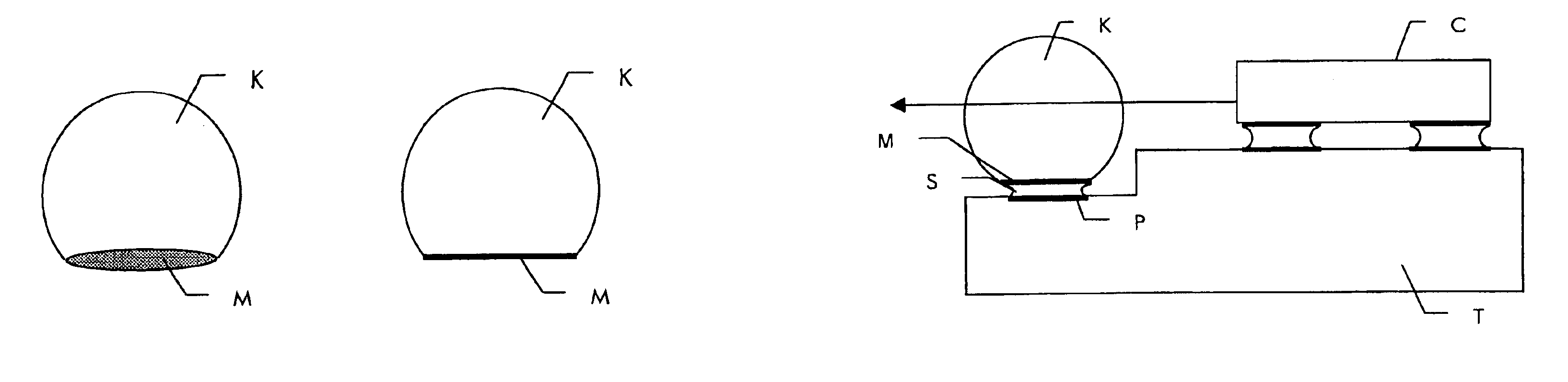
FIG. 1 shows a spherical lens K according to the invention that has a plane surface. Applied to the plane surface is a solderable metal coating M. In the left-hand part of the figure, the spherical lens is shown in a three-dimensional view, while in the right-hand part it is shown in cross section through the centre of the sphere perpendicular to the surface M. The spherical lens comprises a glass such as silica (silicon oxide SiO2). The metal coating comprises a plurality of metal layers, the lowermost being titanium with optionally either gold or a platinum layer on top of it and a gold layer on top of the latter. Other known solderable layer systems are likewise suitable.
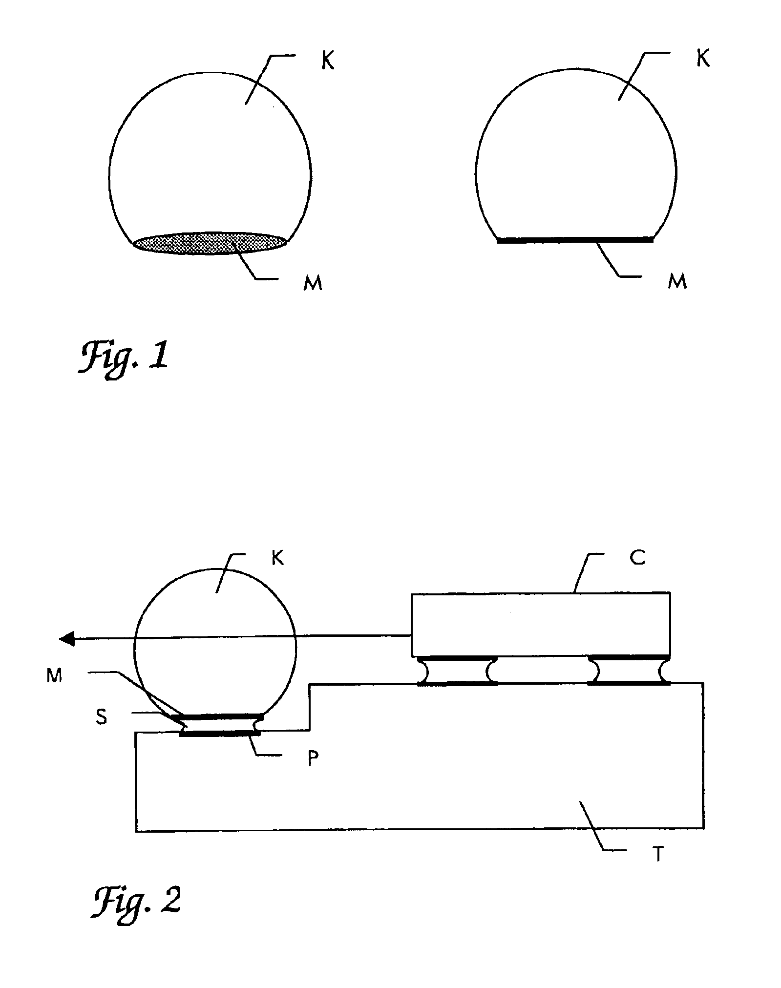
For the purpose of production, a multiplicity of spherical lenses...
PUM
 Abstract
Description
Claims
Application Information