Method for forming SOI substrate

a technology of soi substrate and substrate layer, which is applied in the direction of basic electric elements, electrical apparatus, semiconductor devices, etc., can solve the problems of adversely affecting the quality of the strained silicon channel layer, deterioration of the silicon layer, and generation of lattice defects caused by interface misfit, etc., to achieve improved operational characteristics, low lattice defects, and improved carrier mobility

Inactive Publication Date: 2005-04-19
SAMSUNG ELECTRONICS CO LTD
View PDF10 Cites 28 Cited by
  • Summary
  • Abstract
  • Description
  • Claims
  • Application Information

AI Technical Summary

Benefits of technology

[0018]It is another feature of an embodiment of the present invention to provide methods for forming SOI substrates including forming a strained silicon layer on a SOI layer, which contains a high-concentration of germanium and exhibits low lattice defects, in order to exhibit device characteristics of high carrier mobility.
[0020]In this case, the porous silicon-germanium layer prevents lattice defects of the relaxed silicon-germanium layer from transferring to the silicon-germanium epitaxial layer. As a result, the silicon-germanium epitaxial layer does not suffer from the lattice defects. This makes it possible to form the silicon-germanium layer and the strained silicon layer of the SOI layer without defects.
[0026]The present invention provides methods of forming SOI substrates including forming a strained silicon layer on a SOI layer, which contains a high-concentration of germanium and exhibits low lattice defects, so that semiconductor devices utilizing the SOI substrate formed by the methods of the present invention may exhibit improved operational characteristics due to increased carrier mobility.

Problems solved by technology

Thus, lattice defects caused by interface misfit may be generated in the strained silicon channel layer 16.
Furthermore, removing the phosphorus doped silicon-germanium layer 15 may adversely influence the quality of the strained silicon channel layer 16, where devices will be formed in subsequent processes.
However, if a silicon layer is stacked on the relaxed silicon-germanium layer using an epitaxial growth method, the quality of the silicon layer deteriorates due to lattice defects in the silicon-germanium layer.
Consequently, semiconductor devices using the epitaxial silicon layer may suffer from poor operational characteristics.
Therefore, it undesirable to employ SIMOX when forming an SOI substrate using a silicon-germanium layer having a strained silicon layer.
However, in this method, the silicon-germanium layer 34 disposed under the strained silicon layer 52 may suffer from lattice defects during the hydrogen ion implantation process.
As a result, hydrogen may not properly cure lattice defects of the relaxed silicon-germanium layer.

Method used


Image

  • Method for forming SOI substrate
  • Method for forming SOI substrate
  • Method for forming SOI substrate

Examples


Embodiment Construction

[0031]This application relies for priority upon Korean Patent Application No. 2001-75864, filed on Dec. 3, 2001, “Method For Forming SOI Substrate,” the contents of which are incorporated herein by reference in their entirety.

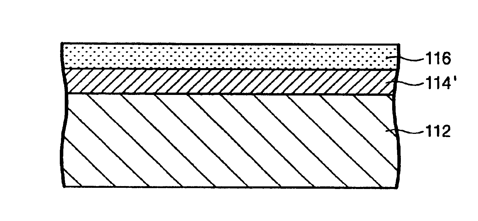
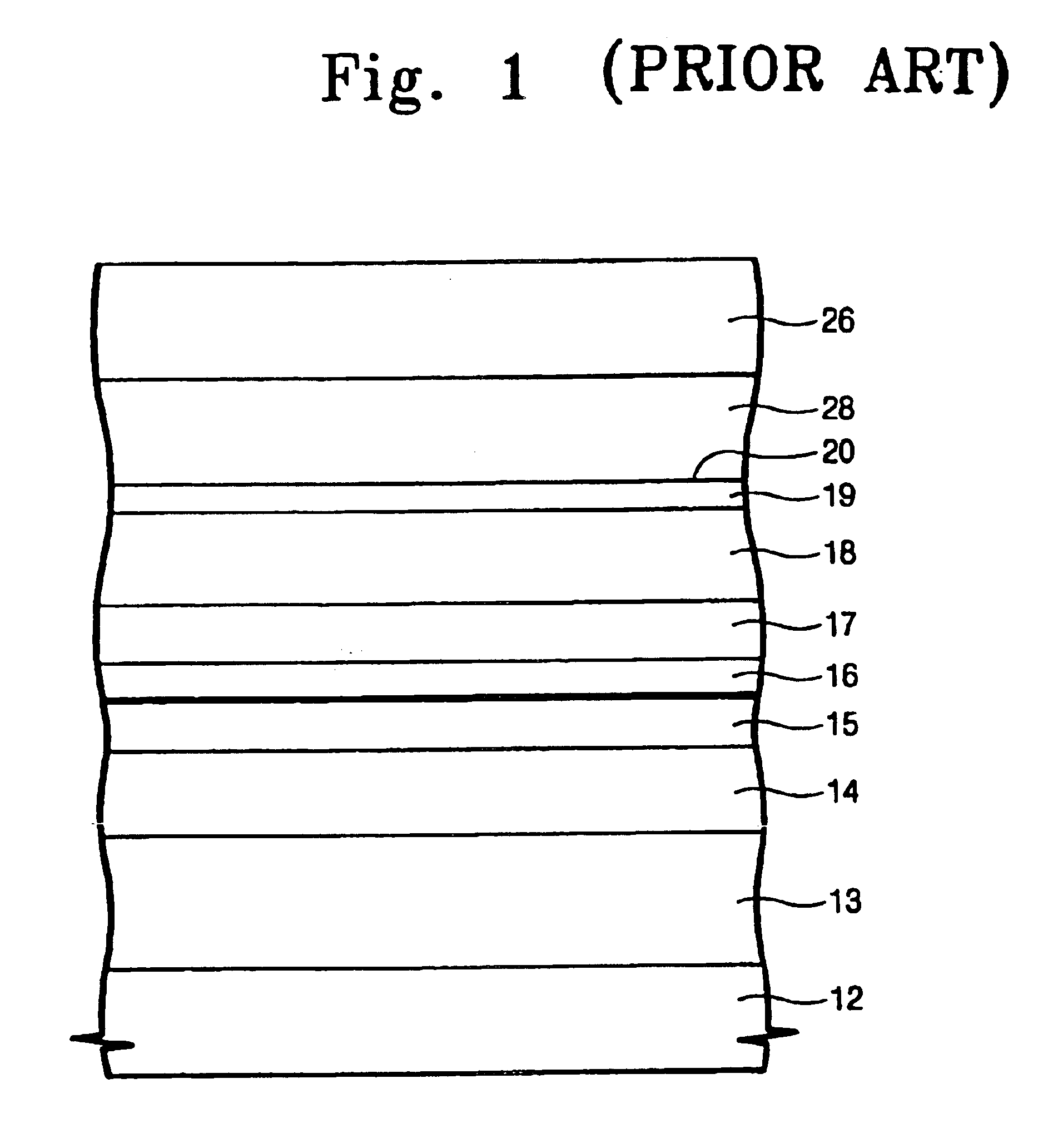
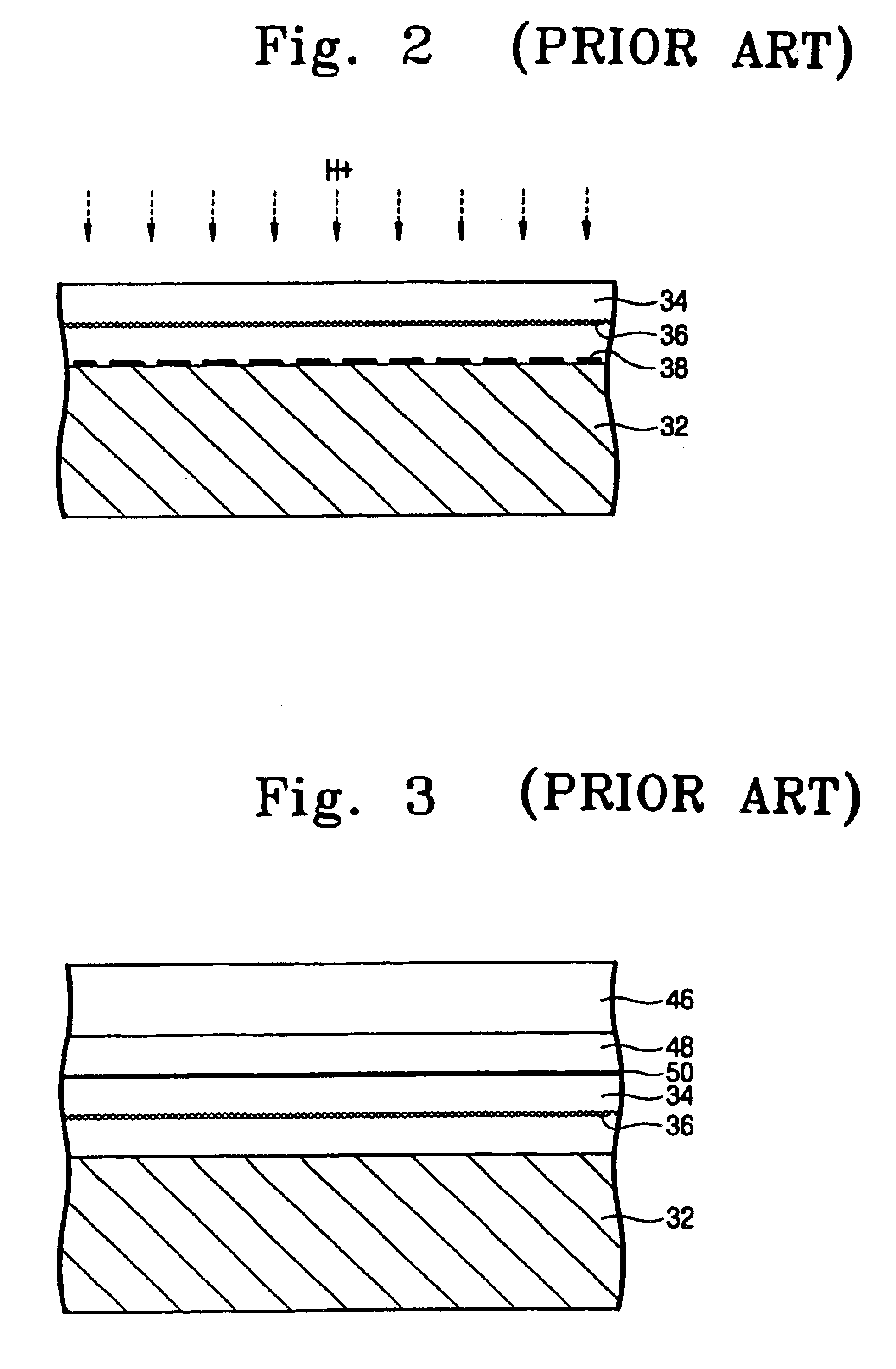
[0032]The present invention will now be described more fully with reference to the accompanying drawings, in which preferred embodiments of the invention are shown. The invention may, however, be embodied in different forms and should not be construed as limited to the embodiments set forth herein. Rather, these embodiments are provided so that this disclosure will be thorough and complete, and will fully convey the scope of the invention to those skilled in the art. In the drawings, the thickness of layers and regions are exaggerated for clarity. It will also be understood that when a layer is referred to as being “on” another layer or substrate, it can be directly on the other layer or substrate, or intervening layers may also be present. Like numbers refer t...


PUM

PropertyMeasurementUnit
thicknessaaaaaaaaaa
thicknessaaaaaaaaaa
thicknessaaaaaaaaaa

Abstract

A method for forming SOI substrates including a SOI layer containing germanium and a strained silicon layer disposed on the SOI layer, comprises forming a relaxed silicon-germanium layer on a first silicon substrate using an epitaxial growth method, and forming a porous silicon-germanium layer thereon. A silicon-germanium epitaxial layer is formed on the porous silicon-germanium layer, an oxide layer is formed on a second silicon substrate, the second silicon substrate is bonded where the oxide layer is formed to the first silicon substrate where the silicon-germanium epitaxial layer is formed. Layers are removed to expose the silicon-germanium epitaxial layer and a strained silicon epitaxial layer is formed thereon. The porous silicon-germanium layer prevents lattice defects of the relaxed silicon-germanium layer from transferring to the silicon-germanium epitaxial layer. Therefore, it is possible to form the silicon-germanium layer and the strained silicon layer of the SOI layer without defects.

Description

BACKGROUND OF THE INVENTION[0001]1. Field of the Invention[0002]The present invention relates to a method for forming a SOI-type substrate. More particularly, the present invention relates to a method for forming a strained silicon layer on a Silicon-germanium On Insulator substrate (hereinafter referred to as “a SOI substrate”).[0003]2. Description of the Related Art[0004]A SOI substrate is obtained by forming a buried oxide layer in a substrate to form a device isolation layer to completely isolate devices from each other. Due to its tolerance to radiation and ability to elevate a breakdown voltage, SOI substrates are mainly used to fabricate semiconductor devices such as high-performance processors.[0005]In case that the SOI substrate includes a SOI layer composed of silicon-germanium and a silicon layer formed on the SOI layer, a difference in lattice constant between the silicon layer and the silicon-germanium layer renders a biaxial tension to the silicon layer. If the silicon...

Claims


Application Information

Patent Timeline
Patent Type & Authority Patents(United States)
IPC IPC(8): H01L21/20H01L21/30H01L21/205H01L21/46H01L27/12H01L21/02H01L21/762
CPCH01L21/76254H01L21/20
Inventor LEE, JUNG-ILFUJIHARA, KAZUYUKILEE, NAE-INBAE, GEUM-JONGRHEE, HWA-SUNGKIM, SANG-SU
Owner SAMSUNG ELECTRONICS CO LTD
Why Eureka
Try Eureka