Semiconductor device package

a semiconductor and device technology, applied in the field of packaging, can solve the problems of easy generation of electromagnetic interference (emi), inability to make thin high frequency circuit substrates b>103/b>, and inability to prevent electric trouble, so as to maintain shielding effect and prevent electric trouble

Active Publication Date: 2005-04-19
NEC COMPOUND SEMICON DEVICES
View PDF13 Cites 68 Cited by
  • Summary
  • Abstract
  • Description
  • Claims
  • Application Information

AI Technical Summary

Benefits of technology

[0019]It is therefore an object of the present invention to provide a semiconductor device package whi...

Problems solved by technology

In such a high frequency oscillator, an electromagnetic interference (EMI) is easily caused by an electric influence from outside.
However, the conventional high frequency semiconductor device package mentioned above has the following problems.
This causes an electric troubl...

Method used


Image

  • Semiconductor device package
  • Semiconductor device package
  • Semiconductor device package

Examples


first embodiment

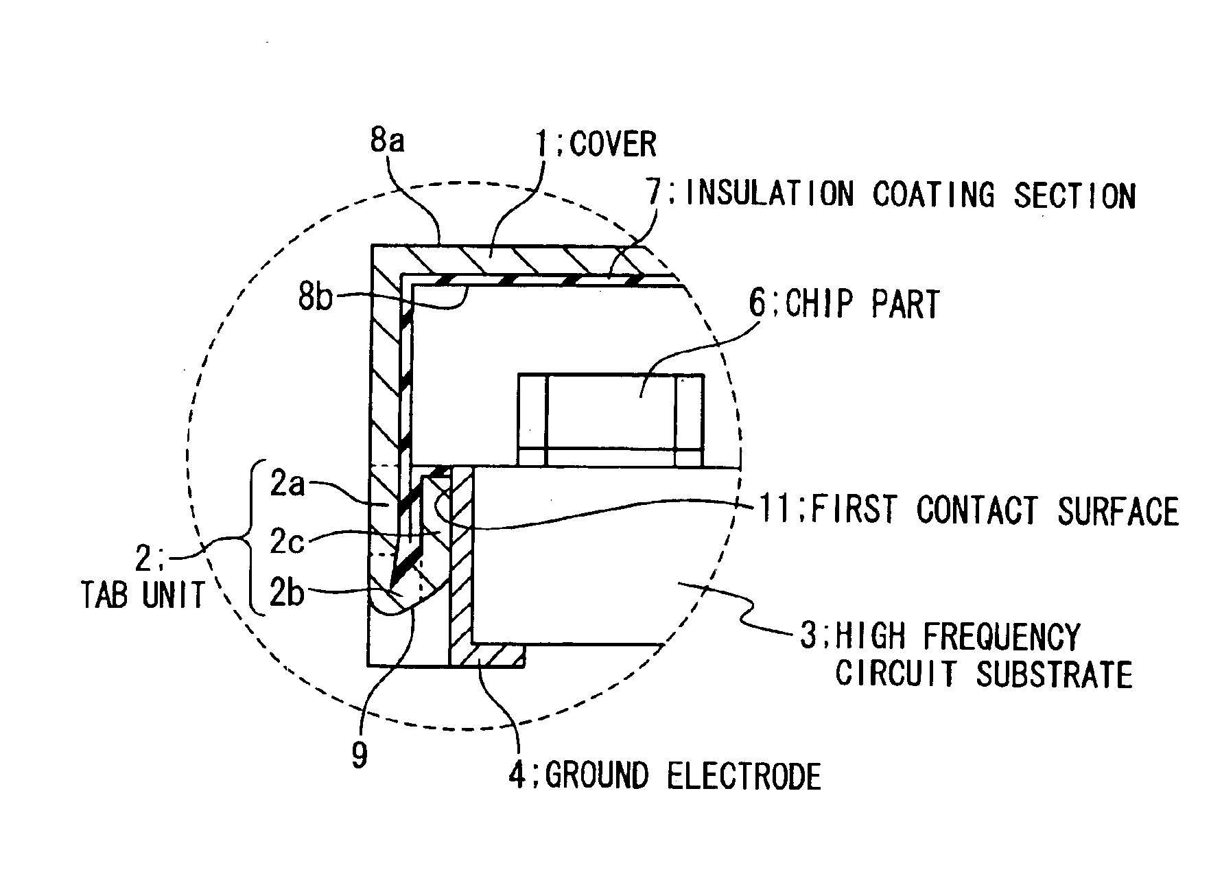
[0042]FIGS. 4 to 6 show a high frequency semiconductor device package according to a first embodiment of the present invention. FIG. 4 is an exploded perspective view of the high frequency semiconductor device package, FIG. 5 is a cross sectional view of the high frequency semiconductor device package, and FIG. 6 is a partially enlarged sectional view of the high frequency semiconductor device package (indicated by a dashed circle).

[0043]The semiconductor device package 10 according to the present invention has a cover 1 and a high frequency circuit substrate 3, to form a shielding case. Also, the semiconductor device package 10 has a device 5 and chip parts 6 formed on the high frequency circuit substrate 3 and accommodated in the shielding case. The device 5 and the chip parts 6 constitute an oscillating circuit. For example, the device 5 includes a FET, and the chip parts include chip condensers, chip resistors, chip inductors and the like

[0044]As shown in FIG. 4, the cover 1 and...

second embodiment

[0057]FIG. 7 shows a high frequency semiconductor device package according to a second embodiment of the present invention. In FIG. 7, the same reference number as in FIG. 6 is given to a structure similar to that in FIG. 6, and a detailed explanation of the structure will be omitted.

[0058]The tab unit 2 has a base section 2a, a bent section 2b and a planar section 2c. The base section 2a and the planar section 2c are formed to be substantially parallel to the side surface of the high frequency circuit substrate 3. The bent section 2b connects the base section 2a and the planar section 2c. In the present embodiment, the tab unit 2 has a “trapezoidal cross section” as shown in FIG. 7. More specifically, the bent section 2b is designed to be straight and forms a first angle θ1 with the base section 2a and a second angle θ2 with the planar section 2c. The first angle θ1 is less than 90 degrees and the second angle θ2 is more than 90 degrees as shown in FIG. 7. Thus, the tab unit 2 beco...

third embodiment

[0062]FIG. 8 shows a high frequency semiconductor device package according to a third embodiment of the present invention. In FIG. 8, the same reference number as in FIG. 6 is given to a structure similar to that in FIG. 6, and a detailed explanation of the structure will be omitted.

[0063]In the present embodiment, the tab unit 2 has a stopper section 2d in addition to the base section 2a, the bent section 2b and the planar section 2c. The base section 2a and the planar section 2c are formed to be substantially parallel to the side surface of the high frequency circuit substrate 3. The bent section 2b connects the base section 2a and the planar section 2c. The planar section 2c has the first contact surface 11 which is contact with the ground electrode 4.

[0064]The stopper section 2d extends from the planar section 2c as shown in FIG. 8. In the present embodiment, the stopper section 2d is formed to be substantially perpendicular to the planar section 2c. Also, the stopper section 2d...


PUM


Abstract

A semiconductor device package includes a substrate, a semiconductor device formed on the substrate, a ground electrode formed on the substrate, a cover designed for covering the semiconductor device, and a tab unit extending from the cover and for holding the substrate. The cover has an outer surface made of conductive material and an inner surface made of insulation material, where the insulating inner surface faces the semiconductor device. The tab unit has a first contact surface which extends from the conductive outer surface and is contact with the ground electrode.

Description

BACKGROUND OF THE INVENTION[0001]1. Field of the Invention[0002]The present invention relates to a package for a high frequency semiconductor device such as a high frequency oscillator (HFO) whose oscillation frequency belongs to, for example, a GHz band. More particularly, the present invention relates to a semiconductor device package, which is designed as a shielding case for surface mounting, for preventing an electromagnetic interference (EMI) and improving a productivity.[0003]2. Description of the Related Art[0004]A high frequency oscillator (HFO) is formed by using a dielectric substance or a strip line and used in, for example, a mobile communications device. In such a high frequency oscillator, an electromagnetic interference (EMI) is easily caused by an electric influence from outside. Therefore, a semiconductor device package is necessary, with which semiconductor devices are encapsulated and shielded.[0005]Japanese Laid Open Utility Model Application (JP-Heisei 1-165650...

Claims


Application Information

Patent Timeline
IPC IPC(8): H01L23/02H01L23/552H05K9/00H01L23/043H01L23/66
CPCH01L23/552H01L23/66H01L2224/48091H01L2224/48227H01L2924/16152H01L24/48H01L2924/19041H01L2924/19105H01L2924/3025H01L2924/1617H01L2924/00014H01L2224/05599H01L2224/45099H01L2224/85399H01L2224/45015H01L2924/207E03D11/00E03D9/00E03D2201/20
Inventor EBIHARA, MASAMI
Owner NEC COMPOUND SEMICON DEVICES
Why Eureka
Try Eureka