Semiconductor device and method of manufacturing the same

a semiconductor device and semiconductor technology, applied in the field of contact methods, can solve the problems of low heat resistance of plastic films, limited processing temperature, and difficulty in directly forming tft over plastic substrates, and achieve the effect of narrowing the frame of a display device and high degree of freedom

Active Publication Date: 2005-04-19
SEMICON ENERGY LAB CO LTD
View PDF6 Cites 22 Cited by
  • Summary
  • Abstract
  • Description
  • Claims
  • Application Information

AI Technical Summary

Benefits of technology

[0036]Miniaturization of total layout area and a module, weight reduction, thinning, narrowing a frame of a display device, or the like can be realized by sequentially laminating a plurality of films to be peeled which are once separately formed over a plastic film or the like. Moreover, reliable contact having high degree of freedom is realized by forming each layer having a connection face of a conductive material and by patterning with the use of a photomask at least having the same pattern. In addition, the layer having a connection face can be used as a wiring layer.

Problems solved by technology

However, compared with glass, quartz, or the like which is generally used as an insulating substrate at present, a plastic film has low heat resistance and has a limitation on processing temperature in a step of forming a TFT.
Therefore, it is difficult to directly form a TFT over a plastic substrate and to obtain high properties.

Method used


Image

  • Semiconductor device and method of manufacturing the same
  • Semiconductor device and method of manufacturing the same
  • Semiconductor device and method of manufacturing the same

Examples


embodiment 1

[0063]A display device using a contacting method of this embodiment mode is described with reference to FIG. 3.

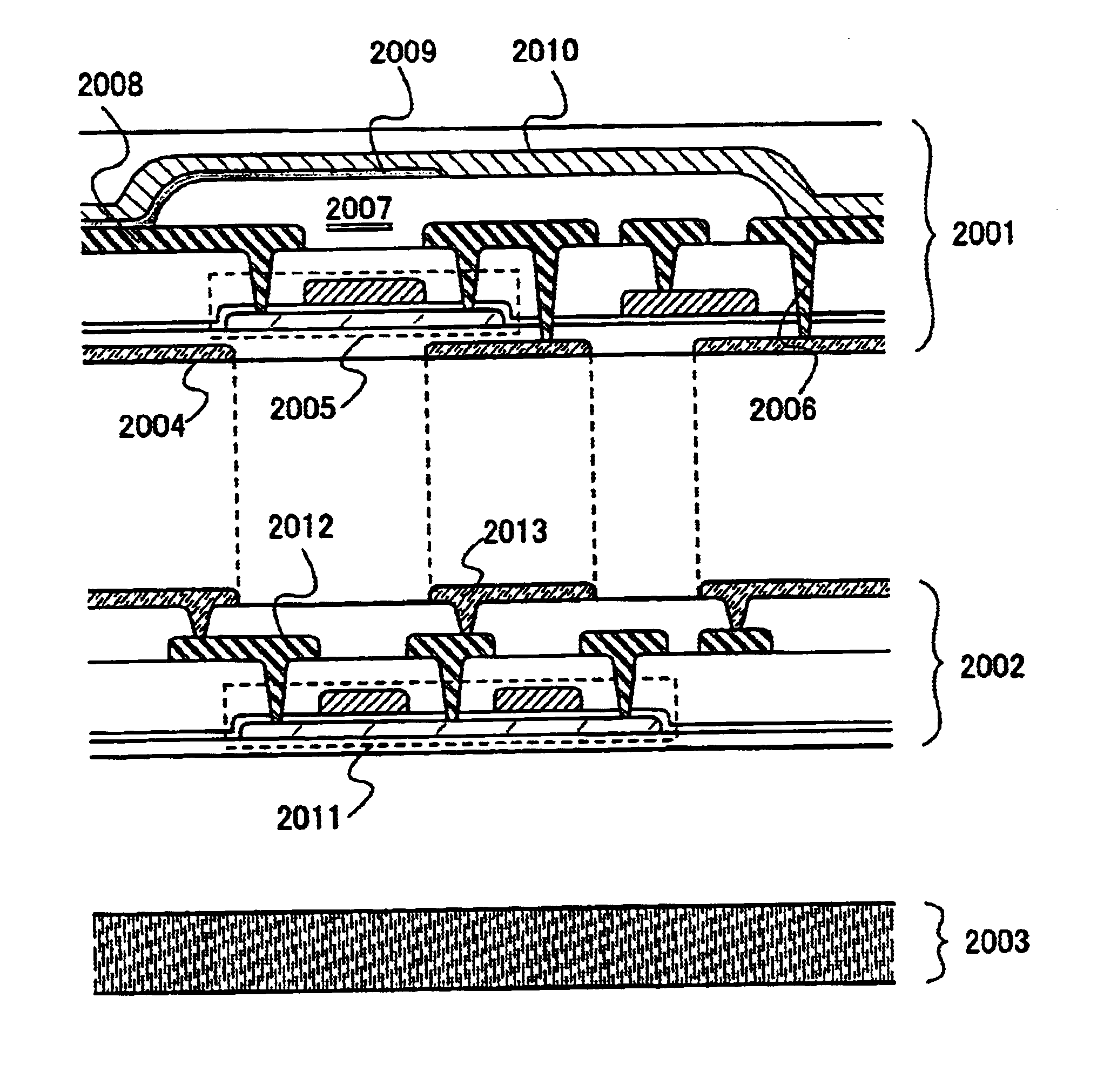
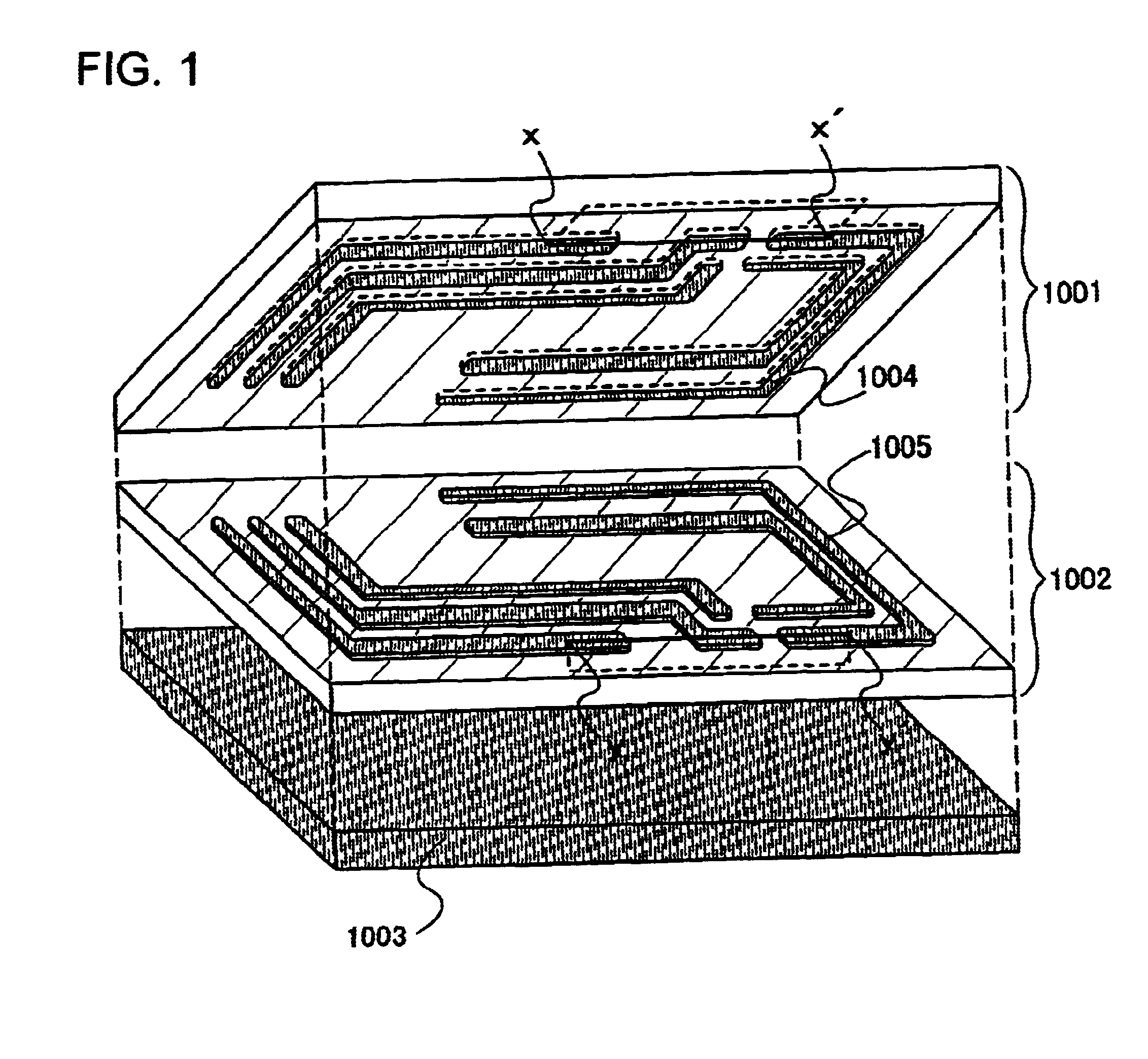
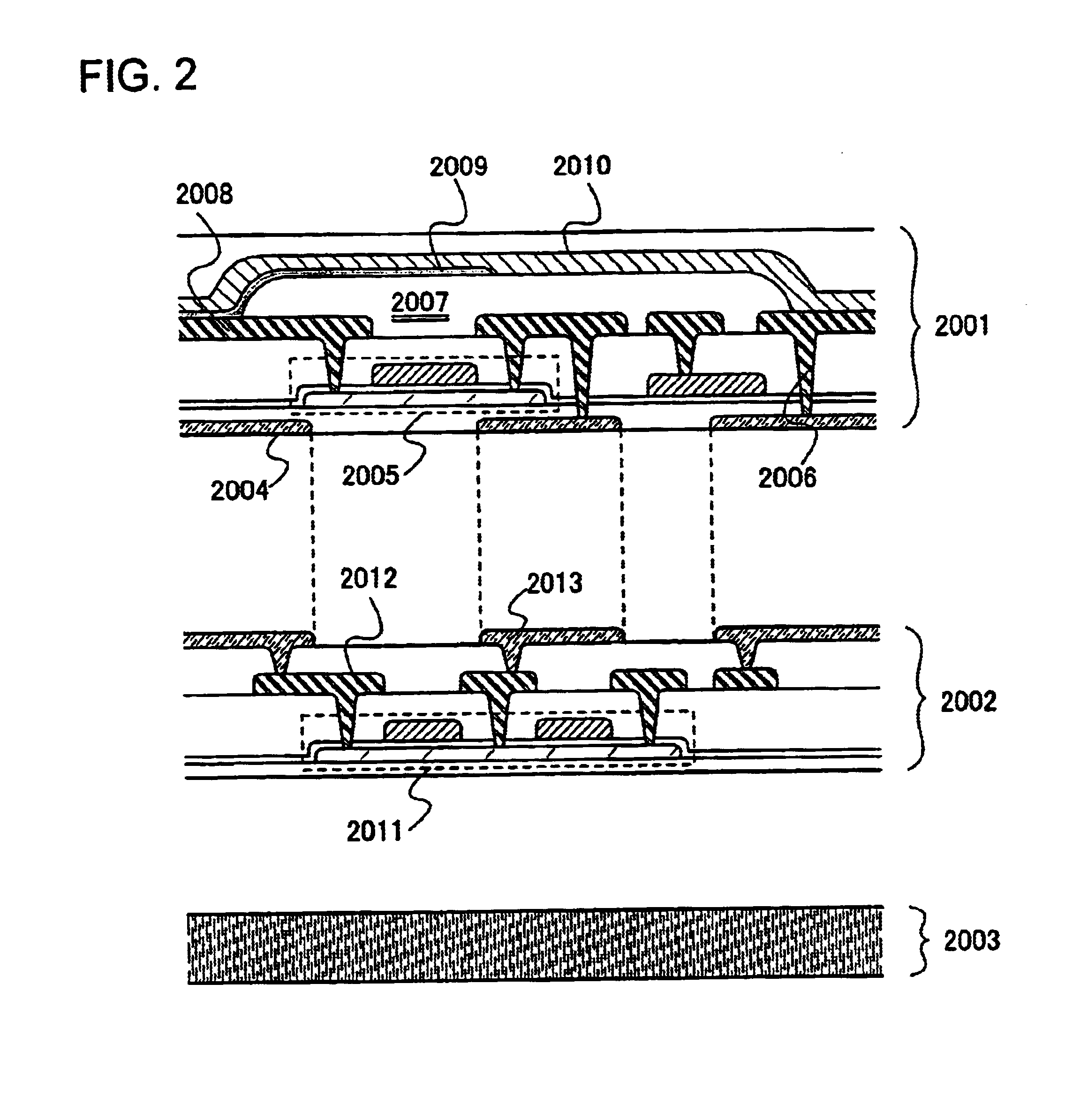
[0064]A film to be peeled C 3003 is a controller portion, which includes a power supply portion 3009 and a signal generating portion 3010. A film to be peeled B 3002 is a driver circuit portion, which includes a first horizontal scanning line driver circuit 3005, a second horizontal scanning line driver circuit 3006, a first vertical scanning line driver circuit 3007, and a second vertical scanning line driver circuit 3008. A film to be peeled A 3001 is a pixel portion, which includes a plurality of pixels 3004 arranged in a matrix.

[0065]At the power supply portion 3009 in the controller portion, each power supply of a desired voltage is generated from a power supply supplied from a battery or an outlet, and is supplied to the driver circuit portion, the signal generating portion 3010, and the like. A power supply, a video signal, a synchronizing signal, and the like are ap...

embodiment 2

[0071]FIG. 5A shows an example of a conventional display device, and FIG. 5B shows an example of a display device using the present invention.

[0072]A general display device has a controller portion, a driver circuit portion, a display portion, and the like. A conventional display device shown in FIG. 5A has a driver circuit portion such as a vertical scanning line driver circuit 5002 and a horizontal scanning line driver circuit 5003, a display portion 5004, and a controller portion 5001 including an IC chip or the like, which are all formed over a glass substrate 5005.

[0073]A display device using the present invention shown in FIG. 5B, has a film to be peeled C 5104 including a controller portion, a film to be peeled B 5103 including a driver circuit portion, and a film to be peeled A 5102 including a display portion 5101 over a plastic substrate 5105. Compared with the conventional display device, the display device using the present invention is effective for miniaturizing the di...


PUM

PropertyMeasurementUnit
conductiveaaaaaaaaaa
insulatingaaaaaaaaaa
semiconductor characteristicsaaaaaaaaaa

Abstract

It is provided a contacting method when a plurality of films to be peeled are laminating. Reduction of total layout area, miniaturization of a module, weight reduction, thinning, narrowing a frame of a display device, or the like can be realized by sequentially laminating a plurality of films to be peeled which are once separately formed over a plastic film or the like. Moreover, reliable contact having high degree of freedom is realized by forming each layer having a connection face of a conductive material and by patterning with the use of a photomask having the same pattern.

Description

TECHNICAL FIELD[0001]The present invention relates to a contacting method among a plurality of films to be peeled, specifically, a contacting method among films to be peeled that include various elements. In addition, the present invention also relates to a semiconductor device having a semiconductor integrated circuit or a thin film transistor (hereinafter, referred to as a TFT) in which a film to be peeled is attached to a substrate and is fixed thereto.[0002]In this specification, the term “semiconductor device” refers to devices that can operate by utilizing semiconductor characteristics. A display device, a semiconductor circuit, and an electronic device using PDP, EL, or liquid crystal are all included in the semiconductor device.BACKGROUND ART[0003]As for a technique for forming a semiconductor integrated circuit, a TFT, or the like over an insulating substrate by using a semiconductor thin film, an attempt to use a flexible substrate typified by a flexible plastic film or th...

Claims


Application Information

Patent Timeline
Patent Type & Authority Patents(United States)
IPC IPC(8): H01L31/18H01L31/036H01L31/0376H01L31/20B32B9/00G02F1/1333H01L21/77H01L27/12H01L27/32H01L51/00
CPCH01L27/1214H01L27/1266G02F1/133305G02F2001/13613H01L2251/5338H01L27/3244H01L51/0024Y10T428/31504G02F1/13613H10K59/12H10K71/50H10K2102/311
Inventor ANZAI, AYAMARUYAMA, JUNYA
Owner SEMICON ENERGY LAB CO LTD
Why Eureka
Try Eureka