High-sensitivity storage pixel sensor having auto-exposure detection

a technology of auto-exposure detection and storage pixel sensor, which is applied in the field of digital cameras, can solve the problems of difficult implementation, limited to either a very slow operation, and the second technique is not good for detecting the exact time, and achieves low noise storage and readout, high sensitivity, and small capacitance

Inactive Publication Date: 2005-04-19
FOVEON
View PDF113 Cites 24 Cited by
  • Summary
  • Abstract
  • Description
  • Claims
  • Application Information

AI Technical Summary

Benefits of technology

[0012]The separation of the photodiode from the charge integration node by the barrier transistor allows high sensitivity, and the separation of the storage node from the charge integration node by the first source-follower transistor allows low noise storage and readout by providing a smaller capacitance for the charge integration node and a larger capacitance for the storage node.

Problems solved by technology

A limitation of these prior pixels storage sensors is the tradeoff that results from the desire for the capacitor to be small to achieve high sensitivity and the competing desire for the capacitor to be large to provide low noise and good storage time.
The first technique is tricky and difficult to implement, since the photocurrents are small and the substrate is large and noisy.
The second technique requires a sequential polling, so is limited to either a very slow operation or to sensing only a very small subset of the pixels.
The second technique is therefore not good for detecting the exact time when a small percentage of pixels are reaching a full-scale exposure.
Such techniques typically sample the image plane at selected fixed points rather than adapting to the lighting conditions of the entire image.
This technique is obviously not as fast, and particularly is unsuited to controlling the exposure time rapidly during a dynamic lighting event, provided for example from a strobe flash.
Mechanical shutters and non-frame-storage electronic sensors cannot be shuttered rapidly enough to use this technique during a flash, which is why the detector is sometimes used to turn off the light source instead of closing a shutter.
These techniques require an awkward coordination between the camera, the light sensor, and the light source, and do not necessarily track automatically the sensitivity (or film speed) and lens aperture of the camera.
These techniques have not been integrated with the use of the overflow current for terminating the exposure time.

Method used


Image

  • High-sensitivity storage pixel sensor having auto-exposure detection
  • High-sensitivity storage pixel sensor having auto-exposure detection
  • High-sensitivity storage pixel sensor having auto-exposure detection

Examples


Embodiment Construction

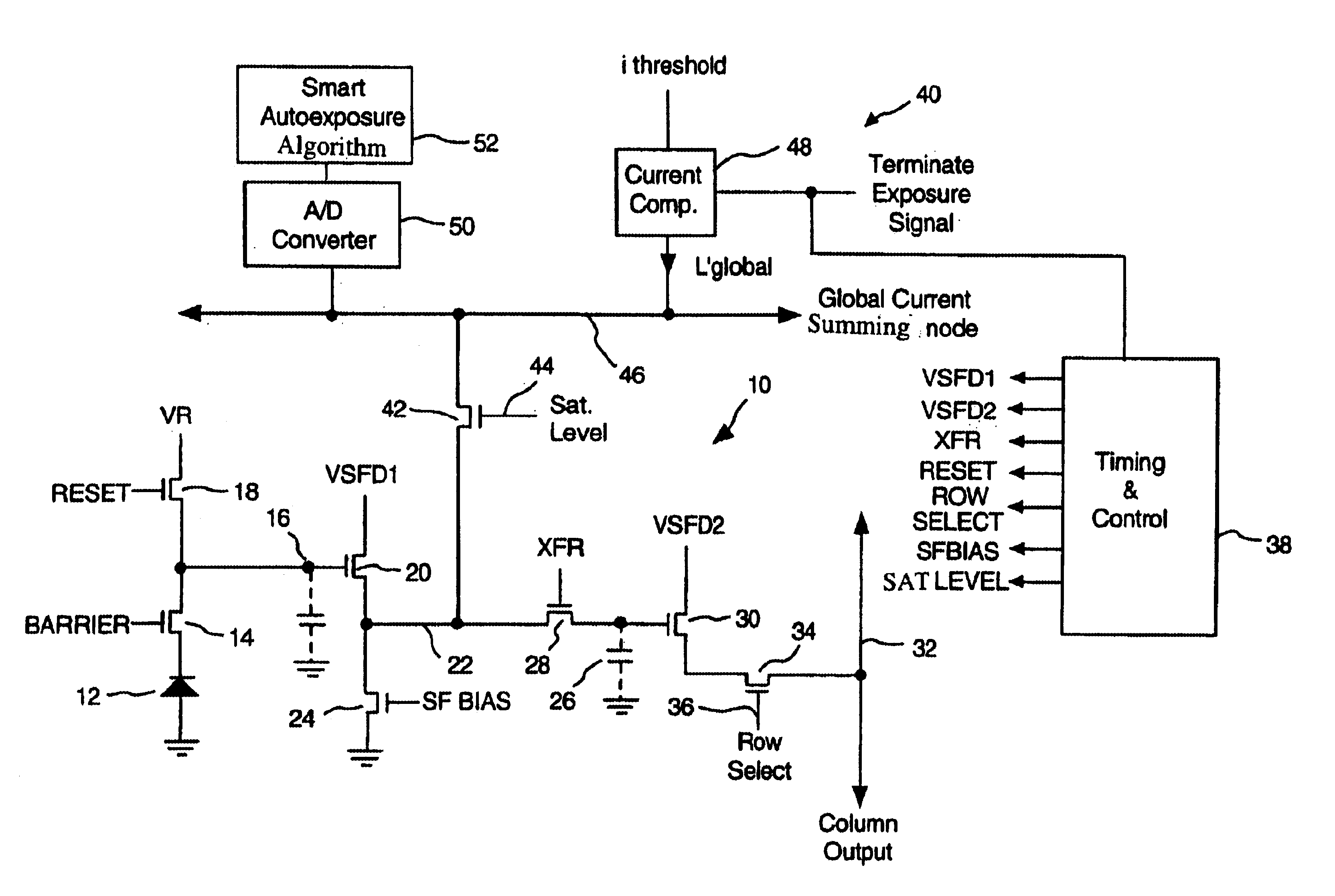
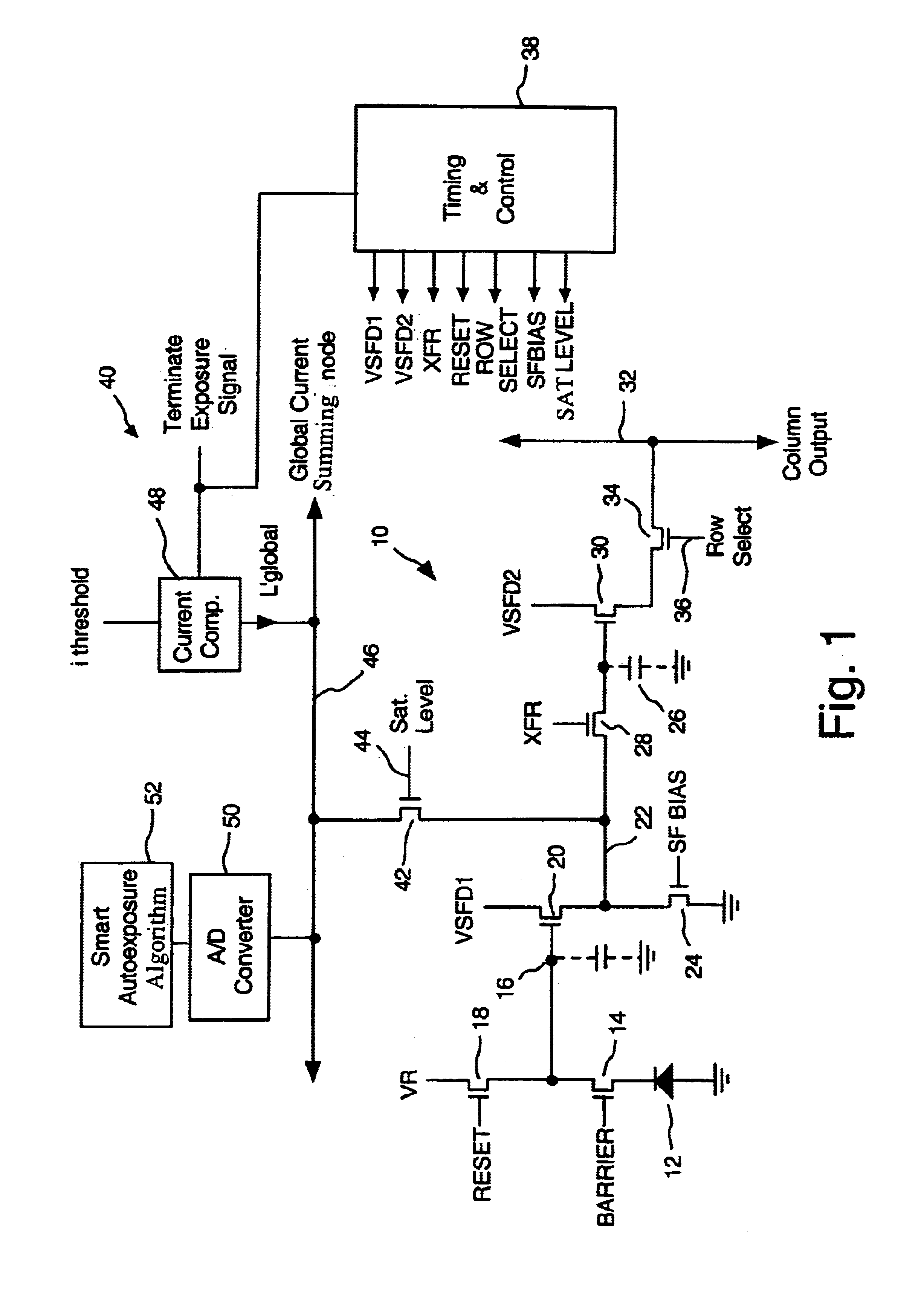
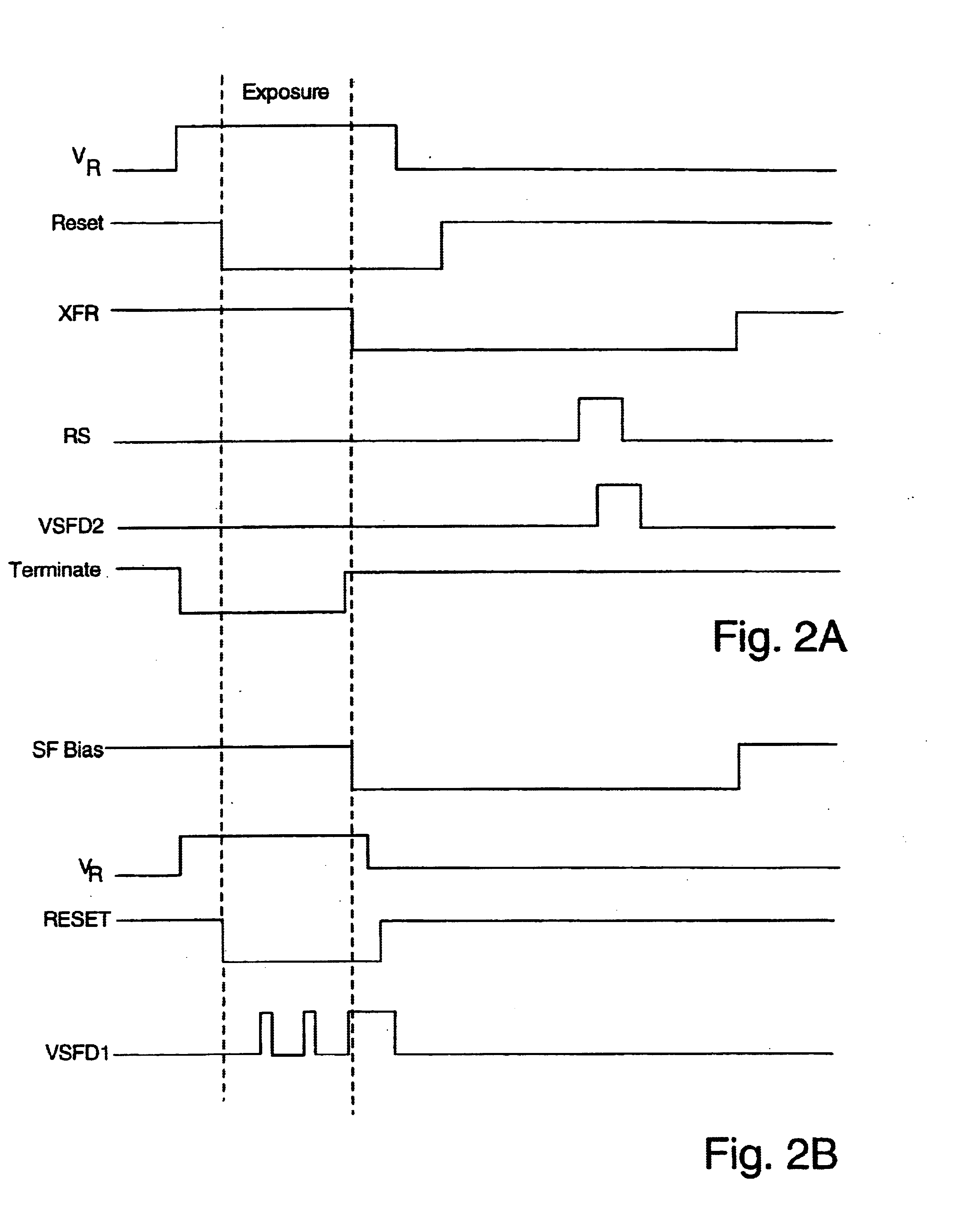
[0018]Persons of ordinary skill in the art will realize that the following description of the present invention is illustrative only and not in any way limiting. Other embodiments of the invention will readily suggest themselves to such skilled persons having the benefit of this disclosure. For example, the illustrative embodiments of the present invention are disclosed using all N-Channel MOS transistor switches, but persons of ordinary skill in the art will appreciate that other technologies could be employed as well. Such skilled persons will readily understand how to adjust the polarities of the various potentials applied to the circuits disclosed herein to implement an embodiment of the present invention employing such other technologies.

[0019]The present invention encompasses various combinations of elements in storage pixel sensors. Different embodiments of storage pixel sensors according the present invention include one or more of the following elements in combination incor...


PUM


Abstract

A storage pixel sensor disposed on a semiconductor substrate comprises a photodiode having a first terminal coupled to a first potential and a second terminal. A barrier transistor has a first terminal coupled to the second terminal of the photodiode, a second terminal and a control gate coupled to a barrier set voltage. A reset transistor has a first terminal coupled to the second terminal of the barrier transistor, a second terminal coupled to a reset reference potential that reverse biases the photodiode, and a control gate coupled to a source of a RESET signal. A photocharge integration node is coupled to said second terminal of said barrier transistor. The photocharge integration node comprises the control gate of a first source-follower transistor. The first source-follower transistor is coupled to a source of bias current and has an output. A capacitive storage node is coupled to the output of the first source-follower transistor and comprises the control gate of a second source-follower transistor having an output. An exposure transistor is coupled between the output of the first source-follower transistor and a global current-summing node and has a control gate coupled to a saturation level voltage.

Description

BACKGROUND OF THE INVENTION[0001]1. Field of the Invention[0002]The present invention relates to digital cameras employing solid-state pixel sensors. More particularly, the present invention relates to improved sensitivity and autoexposure detection apparatus and methods for use in digital cameras.[0003]2. The Prior Art[0004]Storage pixel sensors are known in the art. These devices sense photo-integrated charge stored on a capacitor. A limitation of these prior pixels storage sensors is the tradeoff that results from the desire for the capacitor to be small to achieve high sensitivity and the competing desire for the capacitor to be large to provide low noise and good storage time.[0005]Prior art exposure control techniques known to the inventors that use the actual image sensors during the actual exposure interval are of two types. Some prior art techniques integrate the total photocurrent by a common back-side electrode (anode) of a group of photodiodes—i.e., they integrate the su...

Claims


Application Information

Patent Timeline
Patent Type & Authority Patents(United States)
IPC IPC(8): H04N3/15H04N5/351H04N5/3745
CPCH04N5/2351H04N5/3745H04N5/351H04N23/71H04N25/50H04N25/77
Inventor MERRILL, RICHARD B.TURNER, RICHARD M.DONG, MILTON B.LYON, RICHARD F.
Owner FOVEON
Why Eureka
Try Eureka