Multidomain vertically aligned liquid crystal display device

a vertical alignment and liquid crystal display technology, applied in non-linear optics, instruments, optics, etc., can solve the problems of poor visual angle characteristics of homeotropic type liquid crystal display devices in the halftone display state, and achieve the effect of improving visual angle characteristics

Inactive Publication Date: 2005-04-19
SHARP KK
View PDF5 Cites 10 Cited by
  • Summary
  • Abstract
  • Description
  • Claims
  • Application Information

AI Technical Summary

Benefits of technology

[0012]The protrusion and domain border regulating structure divide an area of each pixel into a plurality of domains. In each domain, the tilt direction of liquid crystal molecules is uniform when a voltage is applied. Since a plurality of domains having various tilt directions are formed, the visual angle characteristics can be improved. The gate bus line prevents leak light to be caused by disturbed alignment of liquid crystal molecules near the flection point of the protrusion. Further, since auxiliary capacitance is formed between the gate bus line and pixel electrode, a voltage fluctuation of the pixel electrode to be caused by a voltage change of the data bus line can be suppressed.

Problems solved by technology

As above, a homeotropic type liquid crystal display device is generally has poor visual angle characteristics in the halftone display state.
The visual angle characteristics of a conventional homeotropic type liquid crystal are poor in the halftone display state, as described above.

Method used


Image

  • Multidomain vertically aligned liquid crystal display device
  • Multidomain vertically aligned liquid crystal display device
  • Multidomain vertically aligned liquid crystal display device

Examples


first embodiment

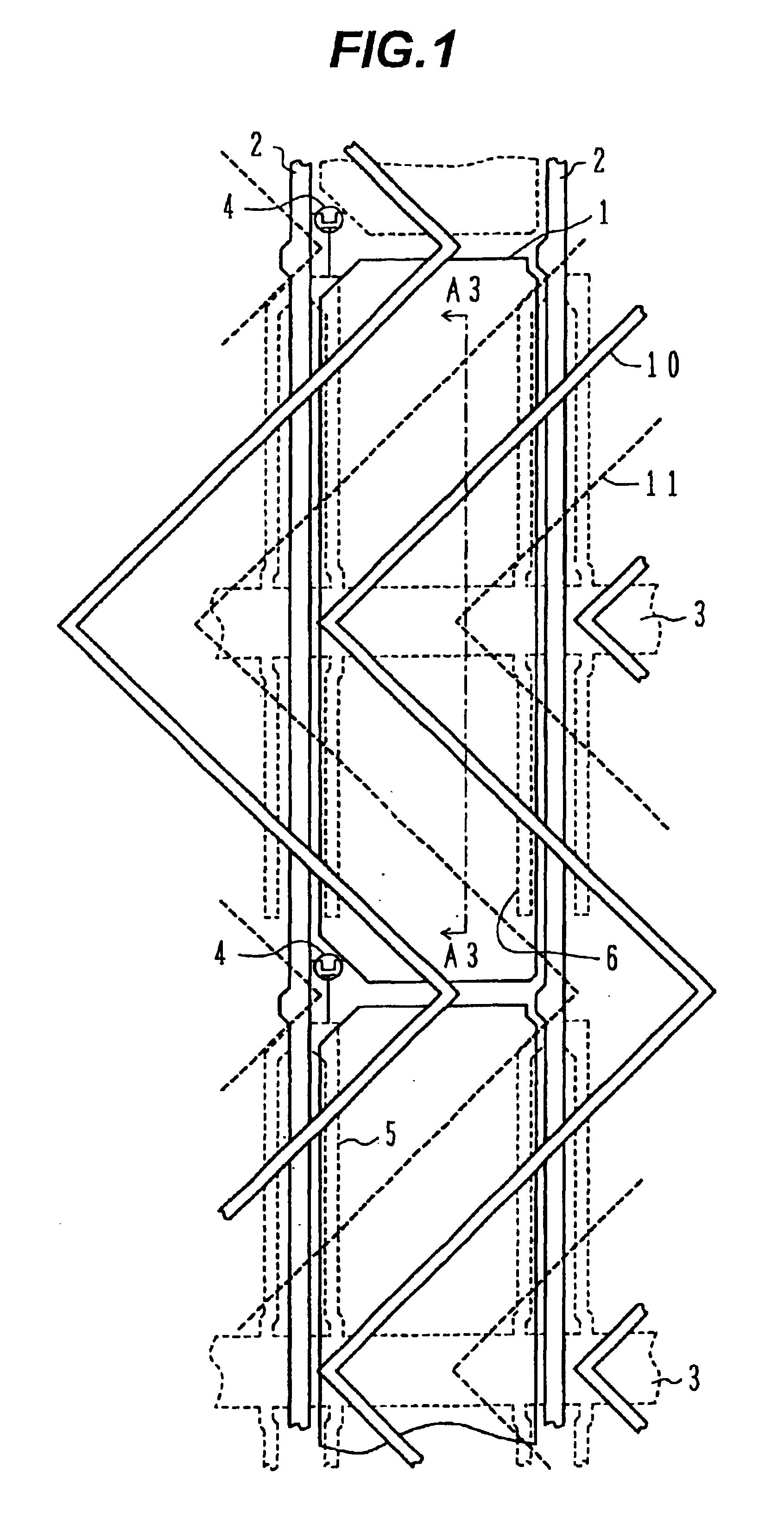
[0054]FIG. 1 is a plan view of a liquid crystal display device according to the invention. A plurality of pixel electrodes 1 are disposed regularly in the row and column directions on a TFT substrate. A data bus line 2 is disposed along each column of the pixel electrodes 1. The data bus line 2 extends in the column direction between two pixels adjacent in the row direction. A gate bus line 3 is disposed along each row of the pixel electrodes 1. The gate bus line 3 extends in the pixel electrodes 1 of the corresponding row, and preferably passes generally at the center of each pixel in the column direction, as viewed along the substrate normal direction.

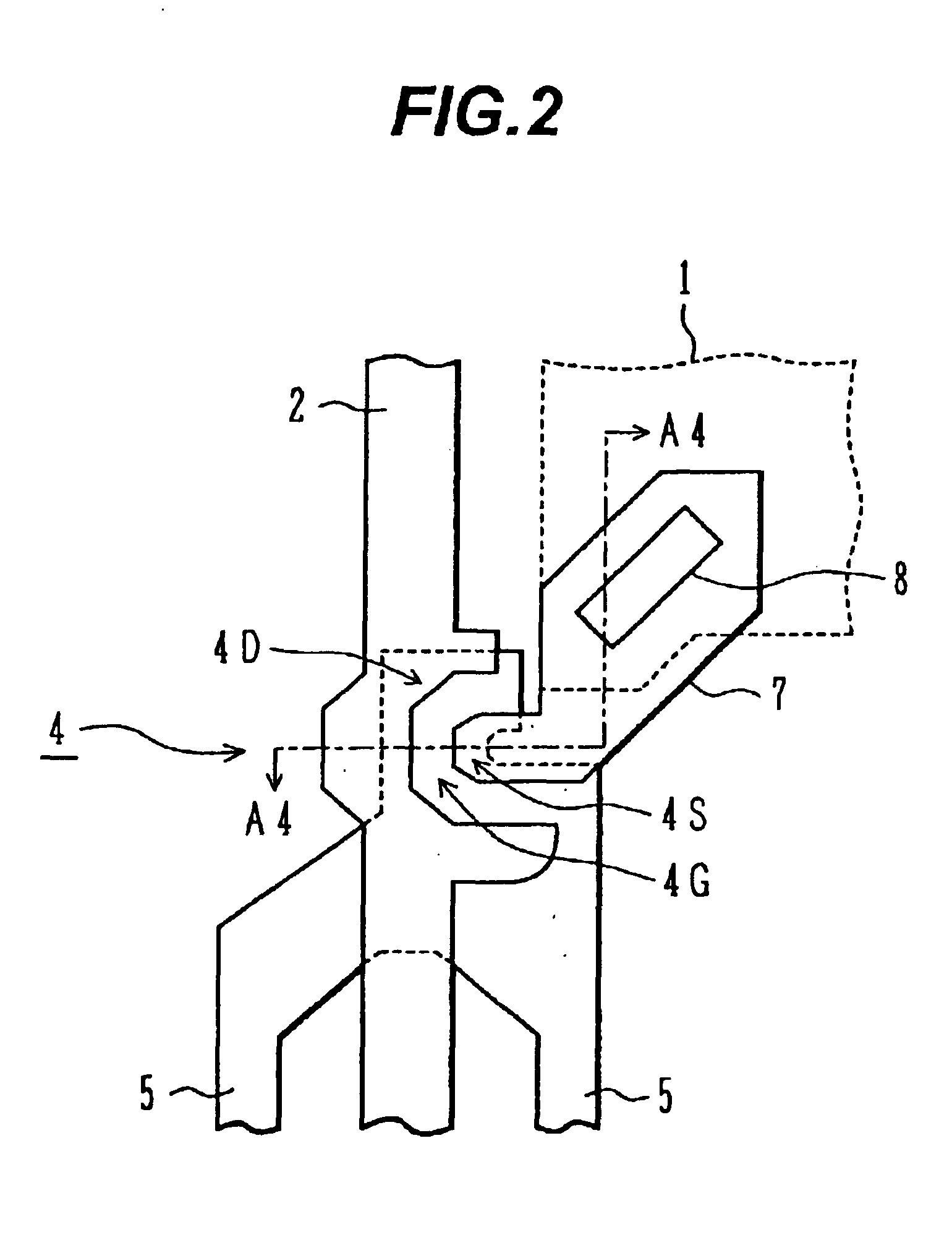
[0055]A TFT 4 is disposed for each pixel electrode 1. TFT 4 connects the pixel electrode 1 and corresponding data bus line 2. The gate electrode of TFT 4 is connected via a gate connection line 5 to the gate bus line 3 corresponding to the row adjacent to the row of the pixel electrode 1 connected to TFT 4. A control signal applied t...

second embodiment

[0081]As in the second embodiment, since the pixel electrode 1 is not disposed under the first protrusion, disturbance of electric lines of force can be alleviated. Since the disturbed alignment area of liquid crystal molecules is localized near the first protrusion 10, the light shielding area can be made small.

[0082]The structure that the slit 1a matching the first protrusion 10 is formed may be applied to the liquid crystal display device previously proposed and shown in FIG. 26. Also in this case, disturbance of the alignment of liquid crystal molecules can be reduced.

[0083]FIG. 6 is a plan view of a liquid crystal display device according to the third embodiment. In the first embodiment, borders of each domain are defined by the first and second protrusions 10 and 11 shown in FIG. 1. In the third embodiment, the second protrusion 11 is not formed on the opposing substrate. In place of the second protrusion 11, slits 20 are formed in the pixel electrode 1.

[0084]As viewed along t...

third embodiment

[0086]As in the third embodiment, since the slits 20 are formed in the pixel electrode 1, an alignment restriction force relative to the liquid crystal molecules in the areas of the slits 20 weakens. Therefore, the domain border can be fixed to the areas of the slits 20.

[0087]Since the slits 20 are formed at the same time when the pixel electrode 1 is patterned, the number of processes does not increase. The second protrusions 11 of the first embodiment are not formed on the opposing substrate. The total number of processes can therefore be reduced.

[0088]FIG. 7 is a plan view of a liquid crystal display device according to the fourth embodiment. Different points from the liquid crystal display device of the third embodiment shown in FIG. 6 will be described.

[0089]In the third embodiment, the gate connection line 5 is disposed along the side of the pixel electrode 1. This layout is used in order to positively form the auxiliary capacitance between the gate connection line 5 and pixel...


PUM

PropertyMeasurementUnit
flection angleaaaaaaaaaa
widthsaaaaaaaaaa
widthsaaaaaaaaaa

Abstract

A pair of substrates is disposed in parallel at a gap distance therebetween. Liquid crystal material containing liquid crystal molecules having negative dielectric anisotropy is filled in between the substrates. The liquid crystal molecules are homeotropically aligned. On the opposing surface of one of the substrates, pixel electrodes are disposed in a matrix form and data bus lines and gate bus lines are disposed. The gate bus line passes an inner area of each pixel electrode. Switching elements are formed on the opposing surface of the substrate. Each switching element is controlled by the gate bus line at another row. Protrusions are formed on the opposing surface of one of the substrates. The protrusions divide an area of the pixel electrode into a plurality of areas and each is bent on the gate bus line. A domain border regulating unit is formed on the opposing surface of the other of the substrates. The protrusions and domain border regulating unit define the borders of each domain.

Description

[0001]This is a divisional of application Ser. No. 09 / 472,328, filed Dec. 23, 1999, now U.S. Pat. No. 6,573,964.[0002]This application is based on Japanese Patent Applications HEI No. 10-371420 filed on Dec. 25, 1999 and HEI No. 10-373058 filed on Dec. 28, 1999, the entire contents of which are incorporated herein by reference.BACKGROUND OF THE INVENTION[0003]a) Field of the Invention[0004]The present invention relates to a liquid crystal display device, and more particularly to a liquid crystal display device wherein liquid crystal molecules are vertically aligned (homeotropic alignment) between opposing substrates when no electric field is applied and one pixel is divided into a plurality of domains.[0005]b) Description of the Related Art[0006]FIGS. 25A to 25C are schematic cross sectional views of a conventional liquid crystal display device of a homeotropic alignment type, respectively illustrating a black display state, a halftone display state, and a white display state. Liqui...

Claims


Application Information

Patent Timeline
Patent Type & Authority Patents(United States)
IPC IPC(8): G02F1/13G02F1/139G02F1/1333
CPCG02F1/1393G02F1/133707
Inventor KAWAI, SATORUKAMADA, TSUYOSHI
Owner SHARP KK
Why Eureka
Try Eureka