Active matrix display and electrooptical device

a technology of active matrix and electrooptical device, which is applied in the direction of semiconductor devices, optics, instruments, etc., can solve the problems of increasing current leaking from the junction, incomplete pn junction, and junction tending to produce leakage current, so as to reduce off current, reduce the effect of electric field strength and greater

Inactive Publication Date: 2005-04-26
SEMICON ENERGY LAB CO LTD
View PDF98 Cites 44 Cited by
  • Summary
  • Abstract
  • Description
  • Claims
  • Application Information

AI Technical Summary

Benefits of technology

[0020]It is not easy to compare the case illustrated in FIG. 2(A) with the case illustrated in FIG. 2(B). In FIG. 2(B), the voltage applied between the source and drain of one TFT is half (or 5 V) of the voltage (10 V) applied in the case of FIG. 2(A). It is unlikely that the voltage between the source and drain is 1 V, unlike the case of TFT 222 shown in FIG. 2(C). This is one advantage of the present invention.
[0021]If LDD regions or offset regions are inserted in the channels of the TFTs 221 and 222, then these regions form drain resistors and source resistors, respectively. This mitigates the electric field strength at the drain junction. Obviously, this reduces the OFF current further.
[0022]If a combination of TFTs and capacitors is added as shown in FIG. 2(D), then greater effect can be produced. However, the rate at which the effect is increased is lower than in the case in which the configuration shown in FIG. 2(A) is replaced by the configuration shown in FIG. 2(C).
[0023]In the above-described structure, the capacitors 223 and 224 can be ordinary capacitors. If one or both of them are MOS capacitors, then integration can be accomplished more efficiently. As mentioned previously, the capacitor 224 is not always necessary. If a lightly doped region is formed between the TFTs 221 and 222 to form a circuit configuration in which a resistor is inserted in series, then the OFF current can be reduced further.
[0024]Each capacitor consists of a fixed capacitor comprising two opposite metal electrodes. Instead, each capacitor may consist of a MOS capacitor formed by laminating a gate-insulating film and a gate electrode on a substantially intrinsic semiconductor film. The MOS capacitor is characterized in that the capacitance is varied by the potential at the gate electrode.
[0025]In one example of the MOS capacitor, three or more TFTs are connected in series with each one pixel electrode. At least one of them excluding those of the series connected TFTs which are located at opposite ends is maintained in conduction and used as a capacitor In another example, a MOS capacitor is connected to the junction of the drain of one of the TFTs connected in series and the source of the other TFT. A stable electrostatic capacitance is obtained by maintaining the gate electrode of the MOS capacitor at an appropriate potential.

Problems solved by technology

Because numerous traps exist in the thin-film transistor, this PN junction is incomplete and so the junction tends to produce a leakage current.
As a result, the electric field is concentrated, so that the current leaking from the junction increases.
These elements hinder transmission of light.
Especially, in a backlit display device comprising an active matrix circuit backlit with intense light, if the aperture ratio is small, a major portion of the incident light is absorbed by TFTs and by the liquid-crystal material and so these TFTs and liquid-crystal material get hot.
As a result, their characteristics are deteriorated.
However, as the image displayed on a liquid crystal display is required to have stricter characteristics, it is more difficult to reduce the OFF current by a required amount by the aforementioned multi-gate method.
However, if more gates are provided, great advantages cannot be expected.

Method used


Image

  • Active matrix display and electrooptical device
  • Active matrix display and electrooptical device
  • Active matrix display and electrooptical device

Examples


example 1

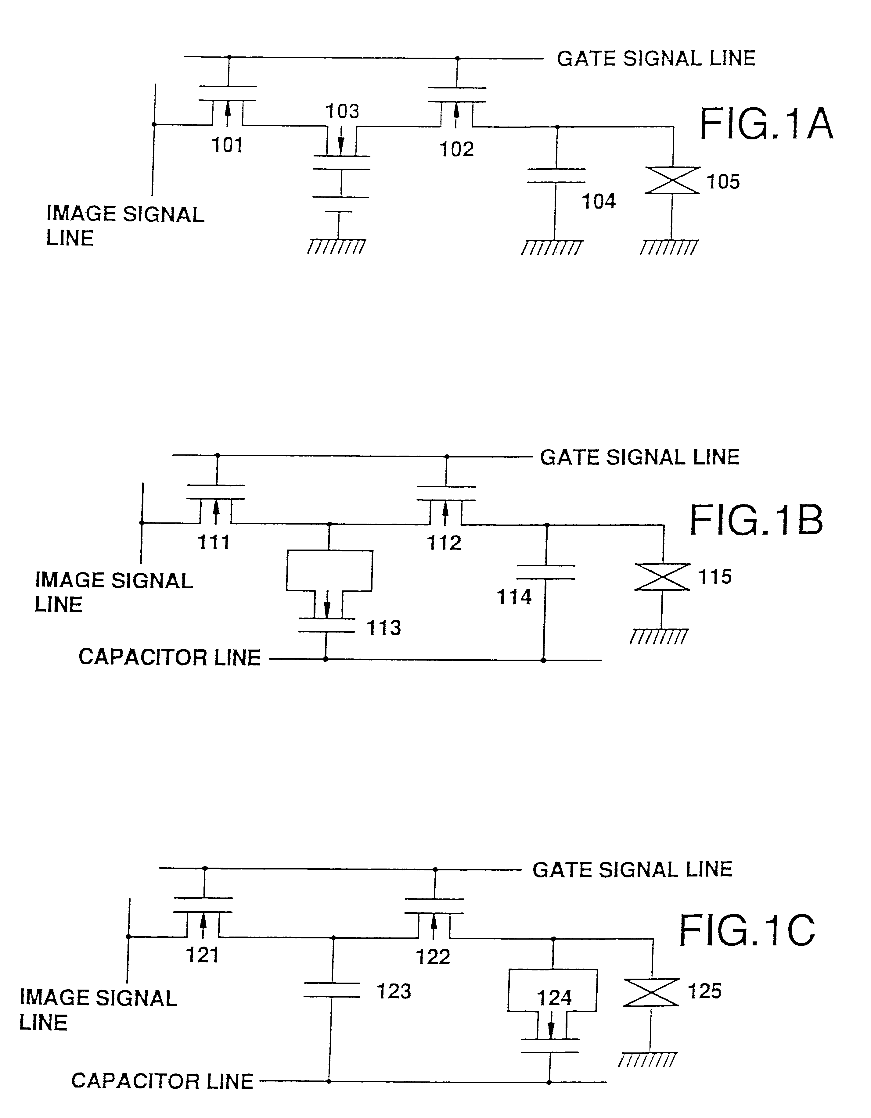
[0056]FIG. 1(a) shows an active matrix display device in which three thin-film transistors (TFTs) are connected with one electrode of one pixel cell 105. All of these TFTs are of the N-channel type. The TFTs can also be of the P-channel type. Where each TFT uses a crystalline silicon semiconductor formed by a low-temperature process, the P-channel type produces smaller OFF current and is deteriorated less easily than the N-channel type.

[0057]Two TFTs 101 and 102 share gate interconnects and are connected with a gate signal line. The source of the TFT 101 is connected with an image signal line. A further TFT 103 which is maintained in conduction is connected between the two TFTs 101 and 102. In order to maintain the TFT 103 in conduction, it is desired to apply a sufficiently high positive potential to the gate so that the TFT 103 is hardly affected by image signal or other signal.

[0058]For example, where the image signal varies from −10 V to +10 V, the gate of the TFT is maintained ...

example 2

[0066]FIG. 1(b) shows an example of pixel of an active matrix circuit in which two TFTs are connected with one pixel electrode. All of the TFTs are of the N-channel type. Similar advantages can be obtained if they are of the P-channel type.

[0067]Two TFTs 111 and 112 share gate interconnects and are connected with a gate signal line. A MOS capacitor 113 is connected between the source and drain of each TFT. The MOS capacitor 113 may be formed by shorting the source of an ordinary TFT to the drain. Since the MOS capacitor uses an N-channel TFT, if the gate is maintained at an appropriate positive potential, the MOS capacitor acts as a capacitor. In order that the MOS capacitor function stably, the potential is preferably maintained at a sufficiently high potential, in the same way as the gate of the TFT 103 of Example 1.

[0068]In order to implement the present invention, it is necessary that the gate of the MOS capacitor 113 be maintained at the aforementioned potential for a major por...

example 3

[0073]FIG. 1(c) shows an example of pixel of an active matrix circuit in which two TFTs are connected with one pixel electrode. All of the TFTs are of the N-channel type. Similar advantages can be obtained if they are of the P-channel type.

[0074]Two TFTs 121 and 122 share gate interconnects and are connected with a gate signal line. A capacitor 123 is connected between the source and drain of each TFT.

[0075]The auxiliary capacitor 124 is formed, using a MOS capacitor. In particular, the auxiliary capacitor 124 is formed by shorting the source of an ordinary TFT to the drain, in the same way as in the case of the MOS capacitor 113 of Example 2. Since this MOS capacitor is composed of an N-channel TFT, if the gate is maintained at an appropriate positive potential, then the N-channel TFT acts as a capacitor. In order that the N-channel TFT act as a capacitor stably, the gate is preferably maintained at a sufficiently high positive potential, in the same way as in the gate of the MOS c...


PUM

PropertyMeasurementUnit
voltageaaaaaaaaaa
voltageaaaaaaaaaa
voltageaaaaaaaaaa

Abstract

A structure for reducing the OFF current of an active matrix display. In the active matrix display, plural TFTs are connected in series with each one pixel electrode. Of these TFTs connected in series, at least one TFT excluding the TFTs located at opposite ends is maintained in conduction. Alternatively, at least one capacitor is connected between the junction of the drain and source of each TFT connected in series and an AC grounded point. Thus, the amount of electric charge released from auxiliary capacitors during cutoff of the TFTs is reduced.

Description

[0001]Divisional of prior Application Ser. No. 09 / 776,933 filed Feb. 7, 2000, now U.S. Pat. No. 6,495,858, which is a continuation of application Ser. No. 08 / 877,307, filed Jun. 17, 1997, now U.S. Pat. No. 6,023,074, which is a divisional application of Serial No. 08 / 456,404, filed Jun. 1, 1995, now U.S. Pat. No. 5,650,636.BACKGROUND OF THE INVENTION[0002]1. Field of the Invention[0003]The present invention relates to an active matrix display construction and, more particularly, to a circuit and device structure for improving the quality of the image displayed on the viewing screen.[0004]2. Description of the Related Art[0005]FIG. 2(A) schematically shows a conventional active matrix display. In this figure, the region 204 surrounded by the broken line is a display region. Thin-film transistors 201 (only one is shown) are arranged in rows and columns in this region 204. Conductive interconnects connected with the source electrodes of the thin-film transistors 201 are image signal li...

Claims


Application Information

Patent Timeline
Patent Type & Authority Patents(United States)
IPC IPC(8): G02F1/13G02F1/1362G09G3/36H01L29/66H01L29/786
CPCG02F1/13624G09G3/3648H01L27/12H01L29/78645H01L29/78696G02F2001/13685G09G2300/0809G09G2300/0819G09G2300/0842H01L27/124G09G2320/0214H01L29/78621G09G2300/0852G02F1/13685
Inventor TAKEMURA, YASUHIKOHAMATANI, TOSHIJIKONUMA, TOSHIMITSUKOYAMA, JUNKAWASAKI, YUJIYAMAZAKI, SHUNPEI
Owner SEMICON ENERGY LAB CO LTD
Why Eureka
Try Eureka