Semiconductor capacitor device having reduced voltage dependence

a capacitor and capacitor technology, applied in the direction of fixed capacitors, stacked capacitors, fixed capacitor details, etc., can solve the problems of difficult to obtain capacitors, and the capacitor structure of the above is not suitable for a highly accurate analog circuit, so as to suppress the voltage dependence of the capacitance valu

Inactive Publication Date: 2005-04-26
SHARP KK
View PDF23 Cites 43 Cited by
  • Summary
  • Abstract
  • Description
  • Claims
  • Application Information

AI Technical Summary

Benefits of technology

[0011]Accordingly, an object of this invention is to provide a semiconductor capacitor device that can suppress the voltage dependence of its capacitance value more than the conventional MIM capacitors.

Problems solved by technology

The PN-junction capacitance is highly dependent upon voltage and therefore it becomes difficult to obtain a capacitor of which the capacitance value does not depend on applied voltage.
Therefore, a capacitor having the above structure is not suitable for a highly accurate analog circuit.

Method used


Image

  • Semiconductor capacitor device having reduced voltage dependence
  • Semiconductor capacitor device having reduced voltage dependence
  • Semiconductor capacitor device having reduced voltage dependence

Examples


Embodiment Construction

[0047]An embodiment of the semiconductor capacitor device of this invention will be described below with reference to the accompanying drawings.

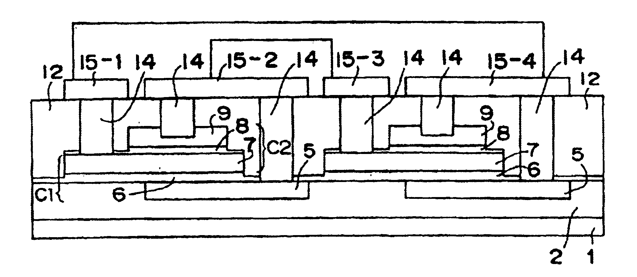
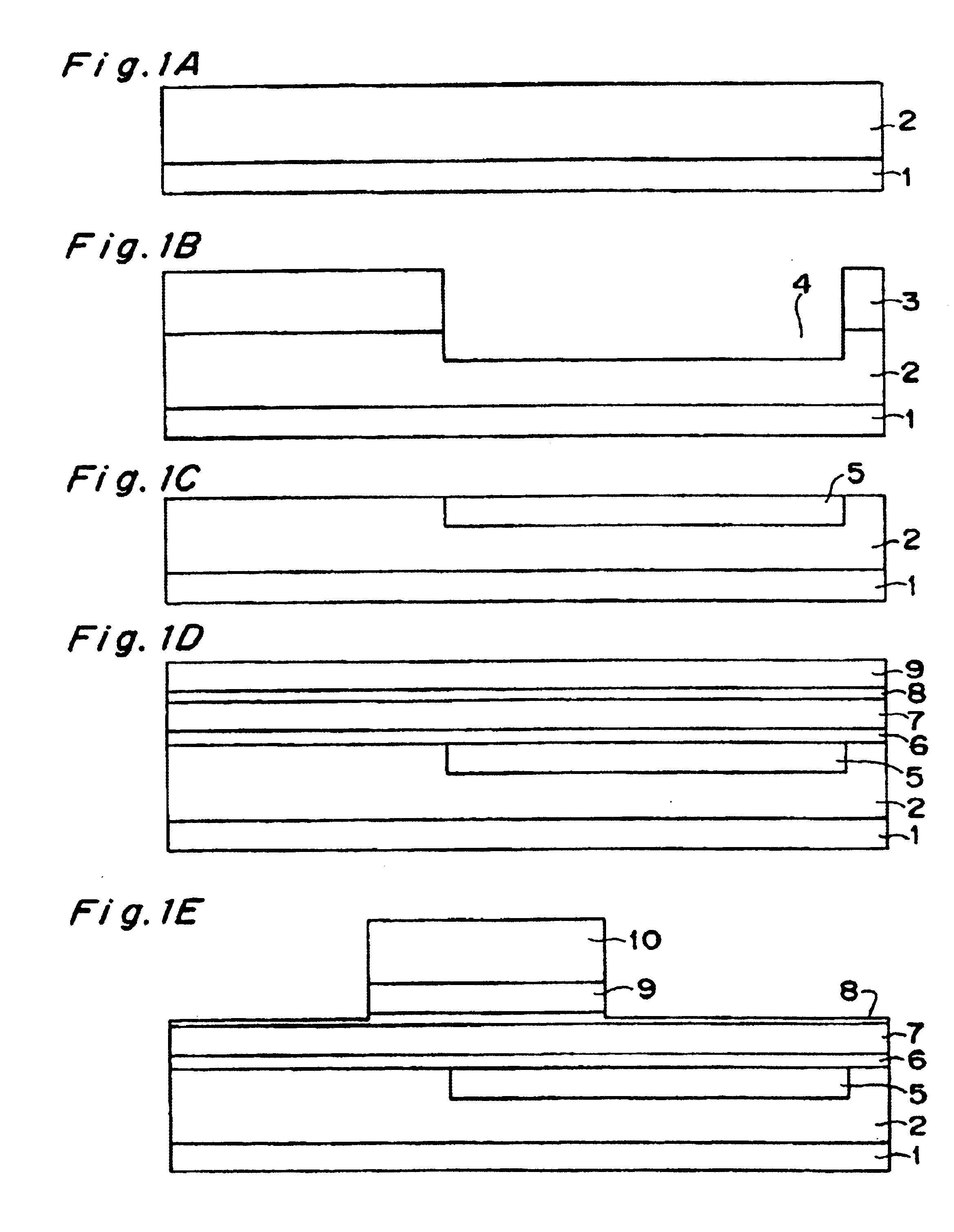
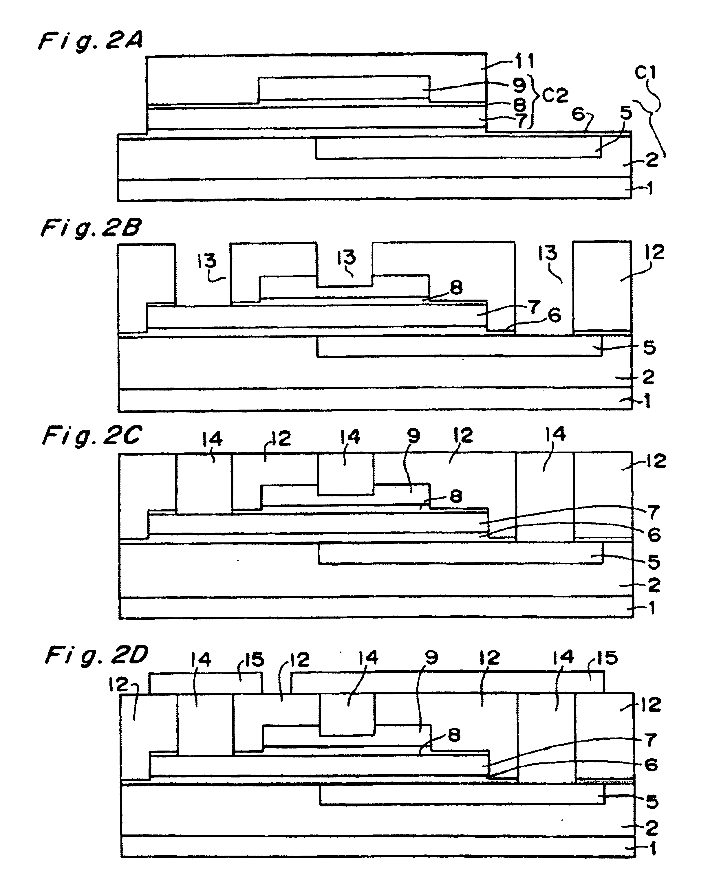
[0048]With reference to FIGS. 1A-1E, FIGS. 2A-2D, and FIG. 3 in order, the process for producing a pair of MIM capacitors in this embodiment will be explained.

[0049]First, as shown in FIG. 1A, after a transistor portion (not shown in the figure) is formed on a semiconductor substrate 1, a first interlayer insulating film 2 is deposited Then, as shown in FIG. 1B, a resist pattern 3 is formed, which is then formed with an opening using a photolithography process. Using this resist pattern 3 as a mask, a surface of the first interlayer insulating film 2 is etched using an anisotropic etching technique and so on to form an approx. 150-300 nm deep groove 4.

[0050]Next, after removing the resist pattern 3, a tungsten film 5 is deposited to a thickness of approx. 500 nm-800 nm on the entire surface of the first interlayer insulating film 2 including...


PUM


Abstract

A semiconductor capacitor device has two pairs of first and second MIM capacitors on a semiconductor substrate. The paired first and second MIM capacitors include respective capacitor dielectric films having different compositions. Also, the paired first and second MIM capacitors are connected in inverse parallel fashion, with an upper electrode of the first MIM capacitor being connected with a lower electrode of the second MIM capacitor and with a lower electrode of the first MIM capacitor being connected with an upper electrode of the second MIM capacitor. Furthermore, the two first MIM capacitors are electrically connected in inverse parallel with each other, and the two second MIM capacitors are also electrically connected in inverse parallel with each other. This arrangement facilitates mutual counteraction of the voltage dependences of the two pairs of first and second MIM capacitors so as to make the voltage dependence of the capacitance of the capacitor device small.

Description

[0001]This is a continuation-in-part application of application Ser. No. 09 / 987,142, filed Nov. 13, 2001 now abandoned.BACKGROUND OF THE INVENTION[0002]This invention relates to a semiconductor capacitor device formed on a semiconductor substrate, in particular to a semiconductor capacitor device that suppresses a change in its capacitance value due to applied voltage.[0003]In a semiconductor capacitor device used for a semiconductor integrated circuit, in particular, for an analog circuit, the capacitance accuracy greatly influences the accuracy of the whole circuit, and thus it is important to suppress a change in capacitance value due to applied voltage.[0004]On the other hand, with miniaturization of semiconductor integrated circuits, an area of a transistor is required to be reduced. Thus, it is also necessary to reduce a capacitor area. For this reason, thinning a capacitor dielectric film has been carried out, but the coefficient of voltage dependence of a capacitance becomes...

Claims


Application Information

Patent Timeline
Patent Type & Authority Patents(United States)
IPC IPC(8): H01L27/08
CPCH01L27/0808
Inventor MORIMOTO, HIDENORI
Owner SHARP KK
Why Eureka
Try Eureka