
Semiconductor device including ternary phase diffusion barrier

a technology of diffusion barrier and semiconductor, applied in the direction of semiconductor devices, semiconductor/solid-state device details, electrical equipment, etc., can solve the problems of degrading the quality of ohmic contact, further increasing resistance, and difficult to minimize the resistance of the wilicide layer, so as to reduce the resistance of an ohmic contact

Inactive Publication Date: 2005-04-26
HYUNDAI ELECTRONICS IND CO LTD
View PDF13 Cites 1 Cited by
  • Summary
  • Abstract
  • Description
  • Claims
  • Application Information

AI Technical Summary

Benefits of technology

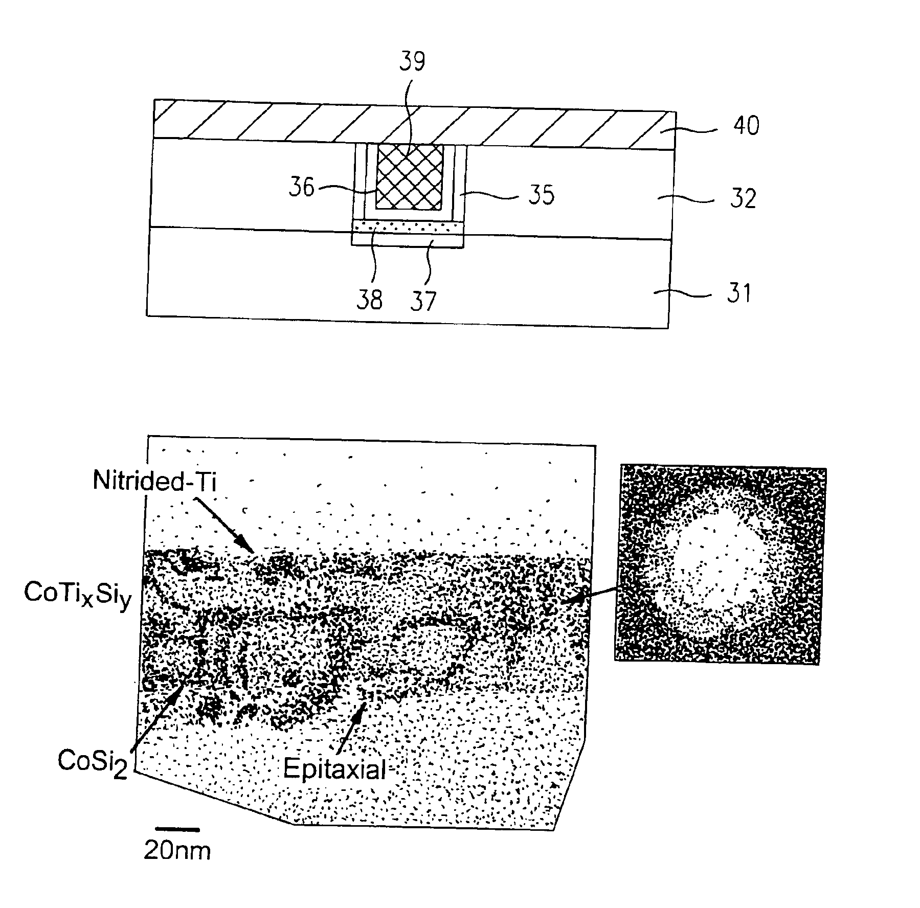
[0022]An object of the present invention is to provide methods for manufacturing a semiconductor device, which simply form a silicide film for reducing a resistance of an ohmic contact between a metal line and a substrate. The method also forms a ternary phase thin film to act as an amorphous diffusion prevention film between a metal line and the silicide film.

Problems solved by technology

First, because the annealing process is performed below 850° C., the silicide film of high resistance is formed. Thus, it is difficult to minimize the resistance of the wilicide layer, i.e., to produce a good ohmic contact.
Second, when compared with the Si, Ti reacts quicker with dopants such as P, As, and B causing dopant loss on the interface between the silicide film and the substrate during the annealing process. This dopant loss results in further increase in resistance, i.e., it degrades the quality of the ohmic contact. Also Ti reacts differently with As, P, and B, resulting in different electrical characteristics in N type and P type substrates.
Third, the silicide film degrades at a temperature of about 750° C. or more. It is difficult to perform annealing process into the silicide film at high temperature due to low thermal stability of the silicide film.
Fourth, since the silicide film is formed unevenly, poor contact occurs.
Thus, it is difficult to effectively prevent the line layer from being diffused into the substrate.
Particularly, TiN is not appropriate for prevention or barrier film of a line layer such as Cu, which is quickly diffused.

Method used


Image

  • Semiconductor device including ternary phase diffusion barrier
  • Semiconductor device including ternary phase diffusion barrier
  • Semiconductor device including ternary phase diffusion barrier

Examples


Embodiment Construction

[0034]Reference will now be made in detail to the preferred embodiments of the present invention, examples of which are illustrated in the accompanying drawings.

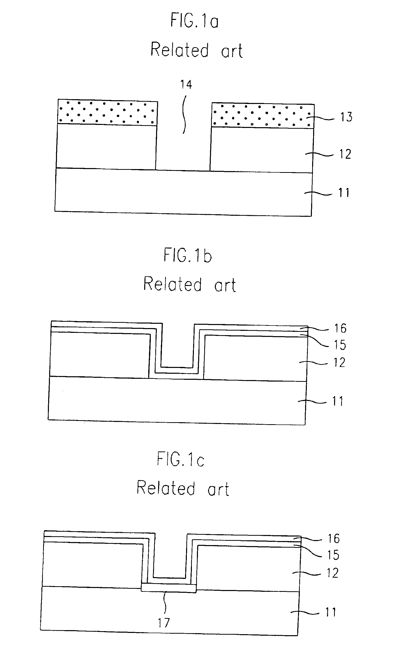
[0035]A method for manufacturing a semiconductor device according to the present invention will be described in detail with reference to the accompanying drawings.

[0036]FIGS. 2a to 2e are sectional views illustrating a method for manufacturing a semiconductor device according to an embodiment of the present invention.

[0037]As shown in FIG. 2a, a CVD oxide film 32 is formed on a semiconductor substrate 31. A photoresist 33 is deposited on the CVD oxide film 32 and then patterned by exposure and developing processes to define a contact region. At this time, instead of the CVD oxide film 32, an inorganic or organic material such as a nitride film may be used.

[0038]Subsequently, the CVD oxide film 32 is selectively removed to partially expose a surface of the semiconductor substrate 31 using the patterned photoresist 33 as a mas...


PUM

PropertyMeasurementUnit
temperatureaaaaaaaaaa
temperaturesaaaaaaaaaa

Abstract

A method for manufacturing a semiconductor device can simply form a silicide film for reducing ohmic contact between a metal line and a substrate and a ternary phase thin film as an amorphous diffusion prevention film between a metal line and the silicide film. The method for manufacturing a semiconductor device includes the steps of sequentially forming a first refractory metal and a second refractory metal on a semiconductor substrate, forming a silicide film on an interface between the semiconductor substrate and the first refractory metal, and reacting the semiconductor substrate with the first and second refractory metals on the silicide film to form a ternary phase thin film.

Description

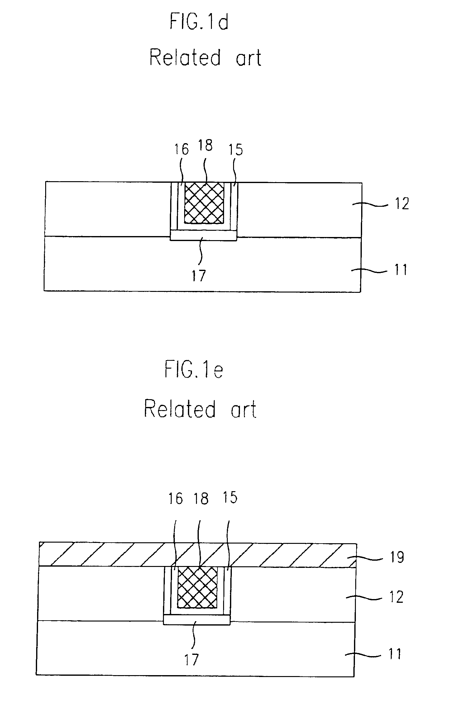
[0001]This application is a Divisional of application Ser. No. 09 / 461,767, filed on Dec. 15, 1999, now U.S. Pat. No. 6,649,520, the entire contents of which are hereby incorporated by reference and for which priority is claimed under 35 U.S.C. §120; and this application claims priority of Application No. 22580 / 1999 filed in Korea on Jun. 16, 1999 under 35 U.S.C. §119.BACKGROUND OF THE INVENTION[0002]1. Field of the Invention[0003]The present invention relates to a method for manufacturing a semiconductor device, and more particularly, to a method for manufacturing a semiconductor device which reduces ohmic contact between a metal line and a substrate.[0004]2. Background of the Related Art[0005]A related art method for manufacturing a semiconductor device will be described with reference to FIGS. 1a to 1e. [0006]As shown in FIG. 1a, a chemical vapor deposition (CVD) oxide film 12 is formed on a semiconductor substrate 11. A photoresist 13 is deposited on the CVD oxide film 12 and the...

Claims


Application Information

Patent Timeline
Patent Type & Authority Patents(United States)
IPC IPC(8): H01L21/28H01L21/285H01L21/768
CPCH01L21/28518H01L21/76843H01L21/76846H01L21/76855H01L21/76856H01L21/76858H01L21/28
Inventor SOHN, DONG KYUNPARK, JI SOOBAE, JONG UK
Owner HYUNDAI ELECTRONICS IND CO LTD
Learn More