Readout circuit with gain and analog-to-digital a conversion for image sensor

a technology of image sensor and readout circuit, applied in the field of image sensor, can solve the problems of low readout rate, low readout rate, and inability to easily adapt to large-scale signal processing, and achieve the effects of reducing bandwidth, reducing various forms of noise from the pixel, and increasing the parallel structure of the overall chip

Inactive Publication Date: 2005-04-26
APTINA IMAGING CORP
View PDF11 Cites 125 Cited by
  • Summary
  • Abstract
  • Description
  • Claims
  • Application Information

AI Technical Summary

Benefits of technology

[0017]Various implementations include one or more of the following advantages. For example, a readout circuit with a variable gain and analog-to-digital conversion can be made sufficiently small, compact and low-powered so that a separate readout circuit can be provided for each column or pair of columns of pixels in an array. Use of the readout circuit, therefore, can increase the parallel structure of the overall chip, thereby reducing the bandwidth which the circuit must be capable of handling.
[0018]Sampling both the reset and signal levels allows correlated double sampling (CDS) to be performed which can reduce various forms of noise from the pixel. Furthermore, sensing charge using an operational amplifier-based integrator circuit allows the pixel values to be read out at a relatively high rate. In addition, the calibration network can help provide more accurate results by correcting various offsets associated with the circuitry and by extending the dynamic range of the analog-to-digital converter

Problems solved by technology

Unfortunately, charge-coupled device (CCD), which have been one of the dominant technologies used for image sensors, do not easily lend themselves to large scale signal processing and are not easily integrated with CMOS circuits.
Moreover, a CCD is read out by sequentially transferring the signal charge through the semiconductor, and the readout rate is limited by the need for nearly perfect charge transfer.
However, in some situations, the output of the CMOS image sensor has a relatively low voltage level due to a low light condition or operation at a high frame rate.
However, in the past, size and power constraints have limited the extent to which such architectures could be implemented for a CMOS imager.

Method used


Image

  • Readout circuit with gain and analog-to-digital a conversion for image sensor
  • Readout circuit with gain and analog-to-digital a conversion for image sensor
  • Readout circuit with gain and analog-to-digital a conversion for image sensor

Examples


Embodiment Construction

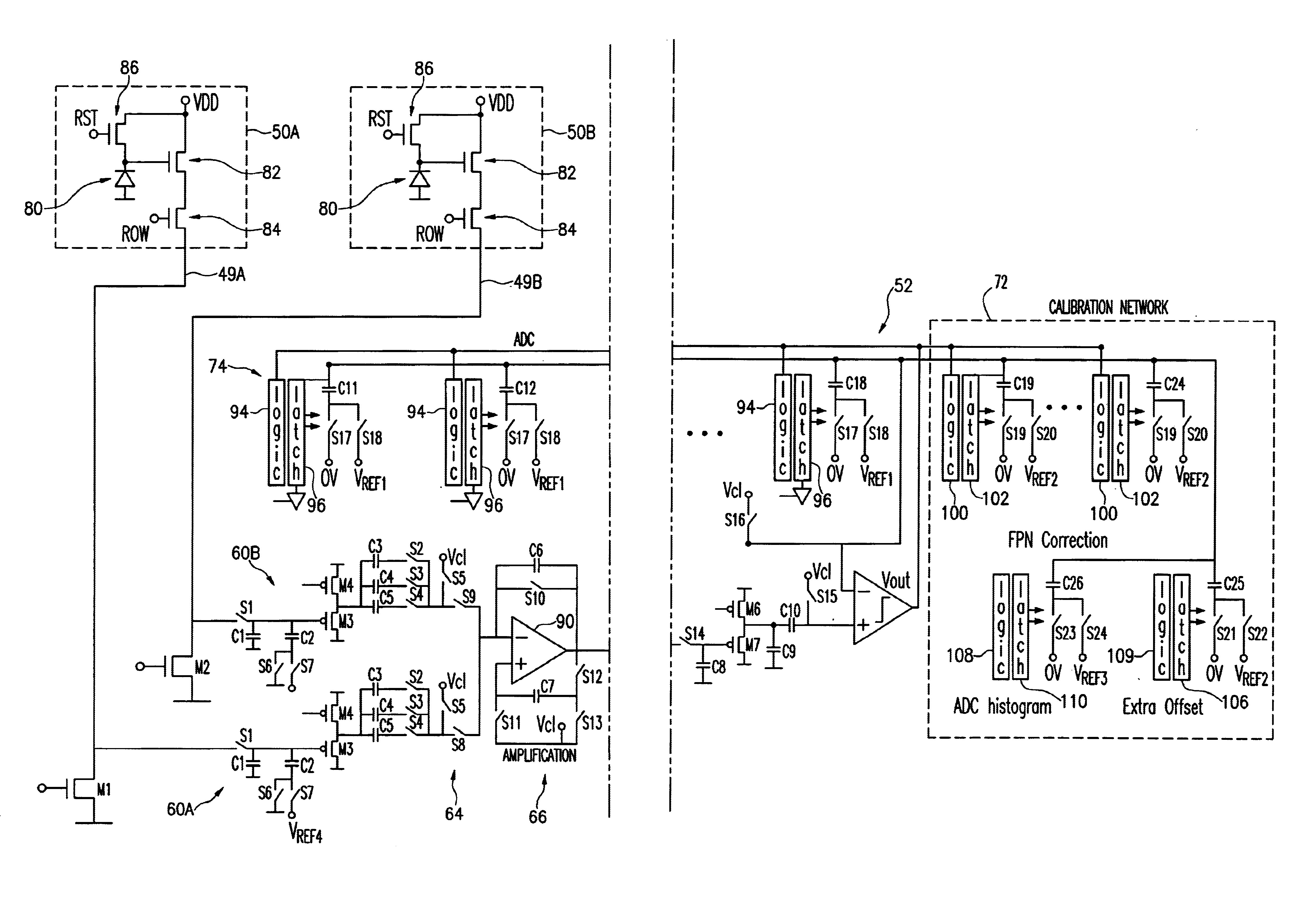
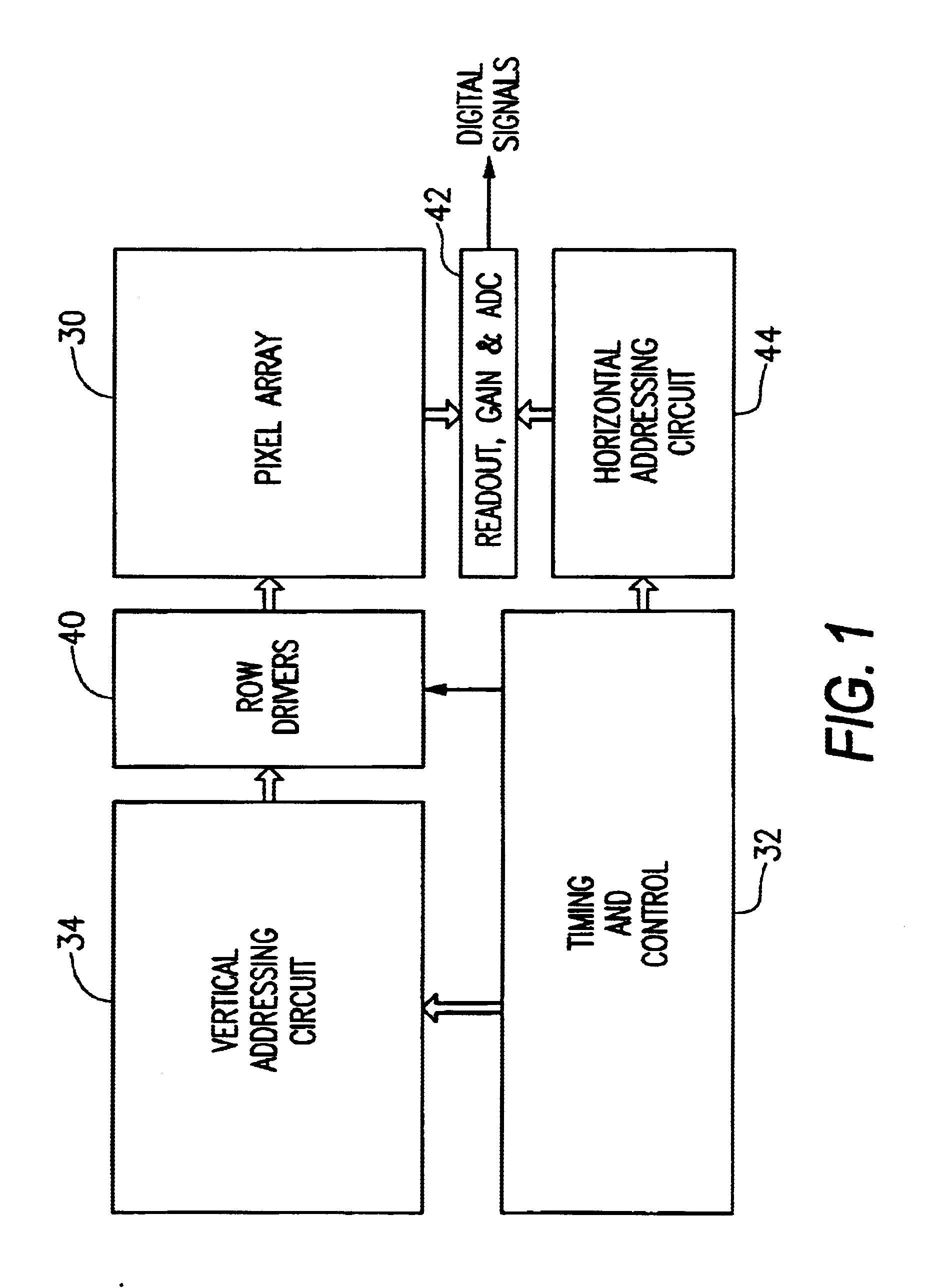
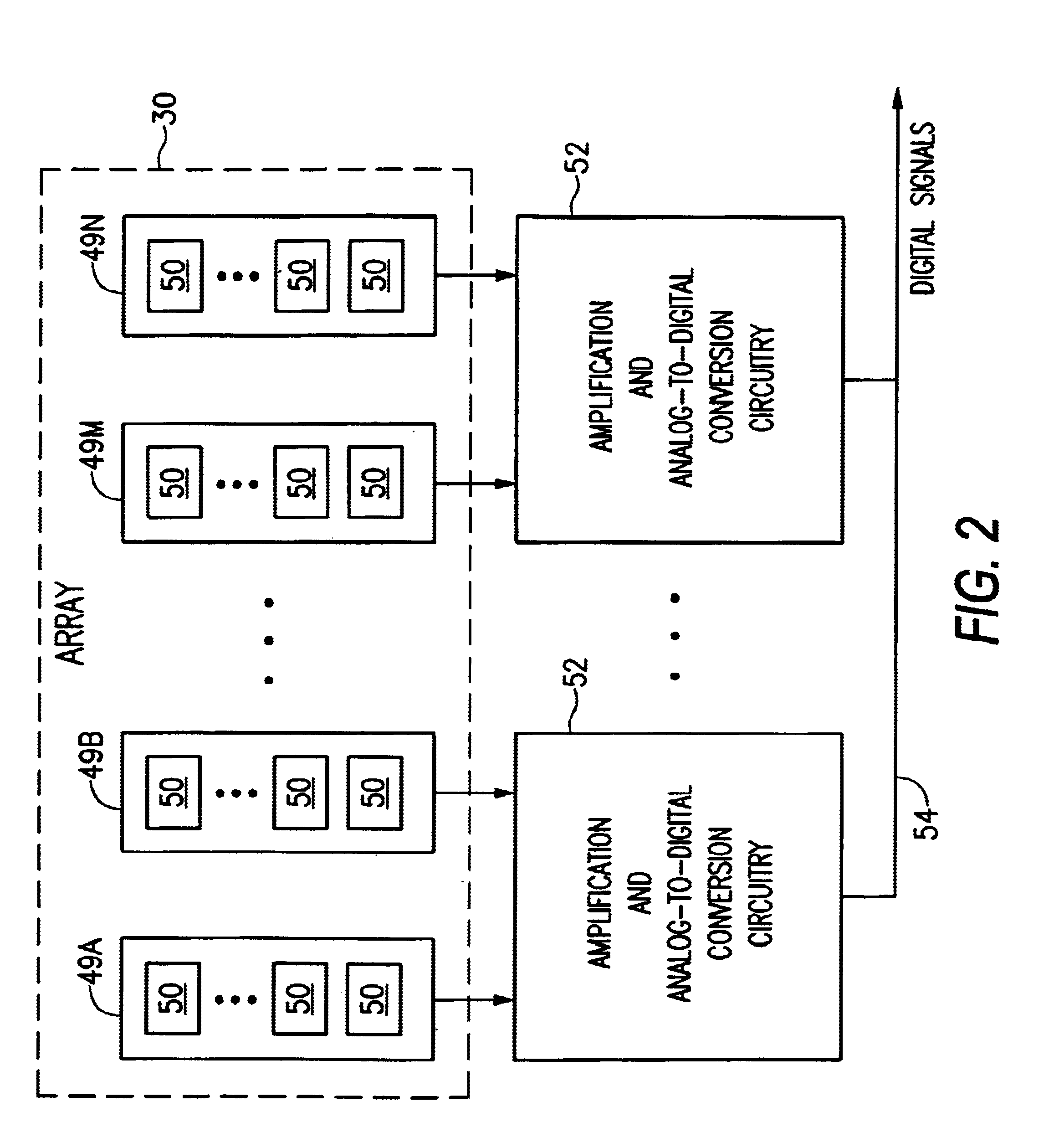
[0035]FIG. 1 shows an exemplary CMOS active pixel sensor integrated circuit chip that includes an array of active pixel sensors 30 and a controller 32 which provides timing and control signals to enable reading out of signals stored in the pixels. Exemplary arrays have dimensions of 128 by 128 pixels or 256 by 256 pixels, although, in general, the size of the array 30 will depend on the particular implementation. The imager is read out a row at a time using a parallel column readout architecture. The controller 32 selects a particular row of pixels in the array 30 by controlling the operation of a vertical addressing circuit 34 and row drivers 40. Signals stored in the selected row of pixels are read out to circuitry 42 for amplifying the pixel signals and for converting the analog signals to corresponding digital signals. Signals for selecting the digital signals corresponding to a particular column in the array are provided from the controller 32 through a horizontal addressing ci...


PUM


Abstract

A CMOS imager includes an array of active pixel sensors, wherein each pixel is associated with a respective column in the array. The imager also includes multiple circuits for reading out values of pixels from the active sensor array. Each readout circuit can be associated with a respective pair of columns in the array and can include first and second sample-and-hold circuits. The first and second sample-and-hold circuits are associated, respectively, with first and second columns of pixels in the array. Each readout circuit also includes an operational amplifier-based charge sensing circuit that selectively provides an amplified differential output signal based on signals sampled either by the first sample-and-hold circuit or the second sample-and-hold circuit. The readout circuit also has an analog-to-digital converter for converting the differential output to a corresponding digital signal using a successive approximation technique. Use of the readout circuit can increase the parallel structure of the overall chip, thereby reducing the bandwidth which each readout circuit must be capable of handling.

Description

[0001]This application claims benefit of U.S. Provisional application 60 / 077,599 filed Mar. 9, 1998.BACKGROUND[0002]This disclosure relates, in general, to image sensors and, in particular, to readout circuits for such sensors.[0003]Image sensors find applications in a wide variety of fields, including machine vision, robotics, guidance and navigation, automotive applications, and consumer products. In many smart image sensors, it is desirable to integrate on-chip circuitry to control the image sensor and to perform signal and image processing on the output image. Unfortunately, charge-coupled device (CCD), which have been one of the dominant technologies used for image sensors, do not easily lend themselves to large scale signal processing and are not easily integrated with CMOS circuits. Moreover, a CCD is read out by sequentially transferring the signal charge through the semiconductor, and the readout rate is limited by the need for nearly perfect charge transfer.[0004]Active pi...

Claims


Application Information

Patent Timeline
Patent Type & Authority Patents(United States)
IPC IPC(8): G11C11/00H01L27/00H03M1/12H04N5/228H04N5/335H04N5/217H04N5/365H04N5/374H04N5/378
CPCH04N5/3575H04N5/378H04N5/363H04N25/616H04N25/65H04N25/75
Inventor PANICACCI, ROGERMANSOORIAN, BARMAKBARNA, SANDORKRYMSKI, ALEXANDER I.
Owner APTINA IMAGING CORP
Why Eureka
Try Eureka