Multi-layered resist structure and manufacturing method of semiconductor device

a manufacturing method and resist technology, applied in the direction of photosensitive materials, instruments, photomechanical equipment, etc., can solve the problems of poor etching resistance of the material per se thinning of the resist pattern has a limit with regard to dry etching resistance, and the pattern failure is ready to occur, so as to avoid the degradation of the patterning precision improve the etching resistance of the upper resist layer. , good adhesive

Inactive Publication Date: 2005-05-03
FUJITSU SEMICON LTD
View PDF17 Cites 7 Cited by
  • Summary
  • Abstract
  • Description
  • Claims
  • Application Information

AI Technical Summary

Benefits of technology

[0013]It is an object of the present invention to provide a multi-layered resist structure capable of suppressing deformation of a pattern of an upper resist layer formed of alicyclic compound, and a semiconductor device manufacturing method employing such multi-layered resist structure.
[0016]Also, the etching resistance of the upper resist layer is good under the etching conditions employed when the intermediate layer is etched by using the pattern of the upper resist layer as a mask.
[0017]Accordingly, the shape of the resist pattern that is obtained by transferring the pattern of the upper resist layer onto the intermediate layer and then transferring the pattern of the intermediate layer onto the lower resist layer becomes good. Thus, the patterning precision of the film using such multi-layered resist can be increased.

Problems solved by technology

However, since the resist pattern is formed to have a narrow width with the higher integration and the miniaturization of the semiconductor device, an aspect ratio that represents a ratio of a height to a width becomes large and then the resist pattern falls down, so that the pattern failure is ready to occur.
In this case, the thinning of the resist pattern has a limit with regard to the dry etching resistance.
It may be considered as the cause of such deformation of the upper resist layer that the etching resistance of the material per se of the upper resist layer is not good in etching the intermediate layer and that the adhesiveness of the upper resist layer to the intermediate layer is not good.

Method used


Image

  • Multi-layered resist structure and manufacturing method of semiconductor device
  • Multi-layered resist structure and manufacturing method of semiconductor device
  • Multi-layered resist structure and manufacturing method of semiconductor device

Examples


Embodiment Construction

[0021]Therefore, an embodiment of the present invention will be explained with reference to the accompanying drawings hereinafter.

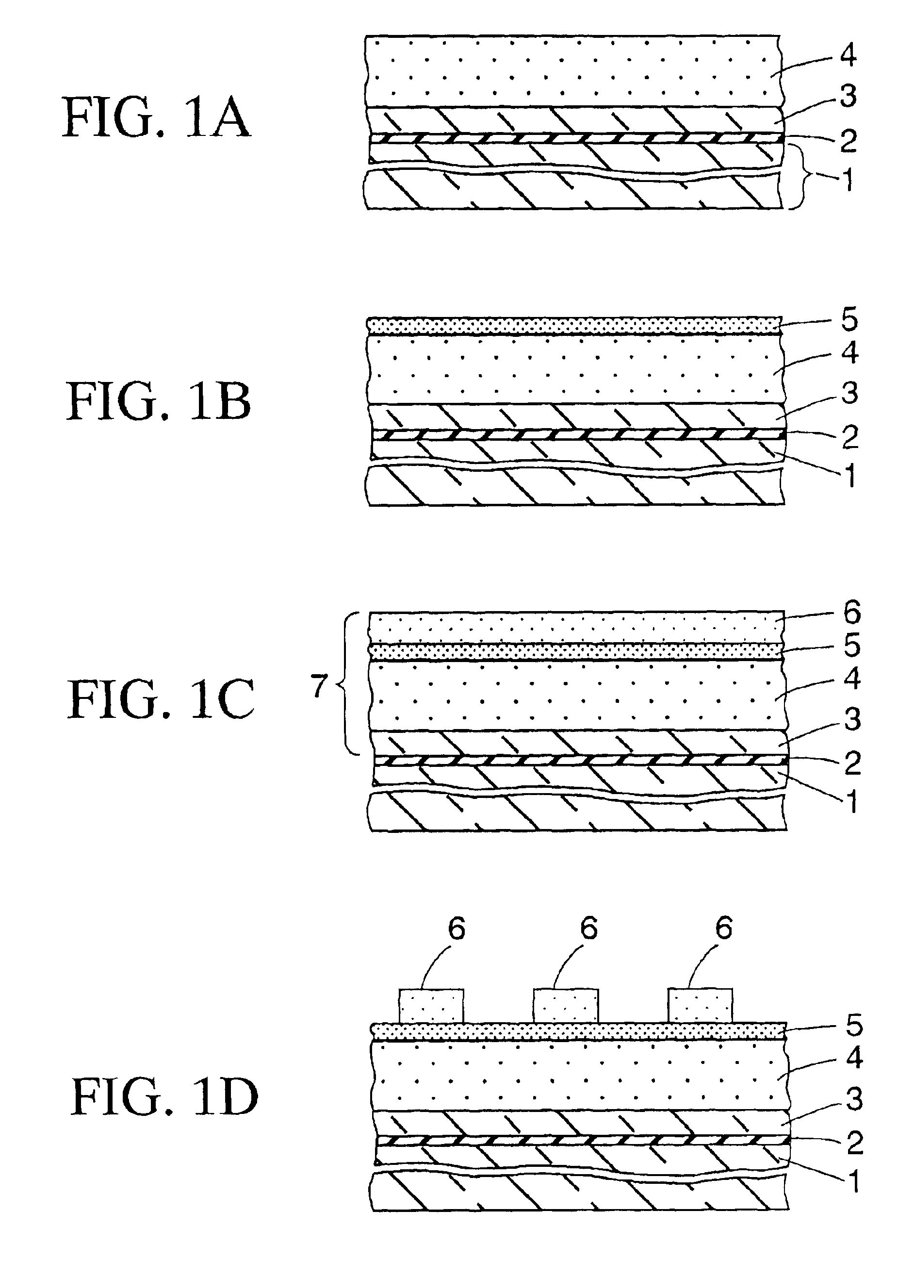
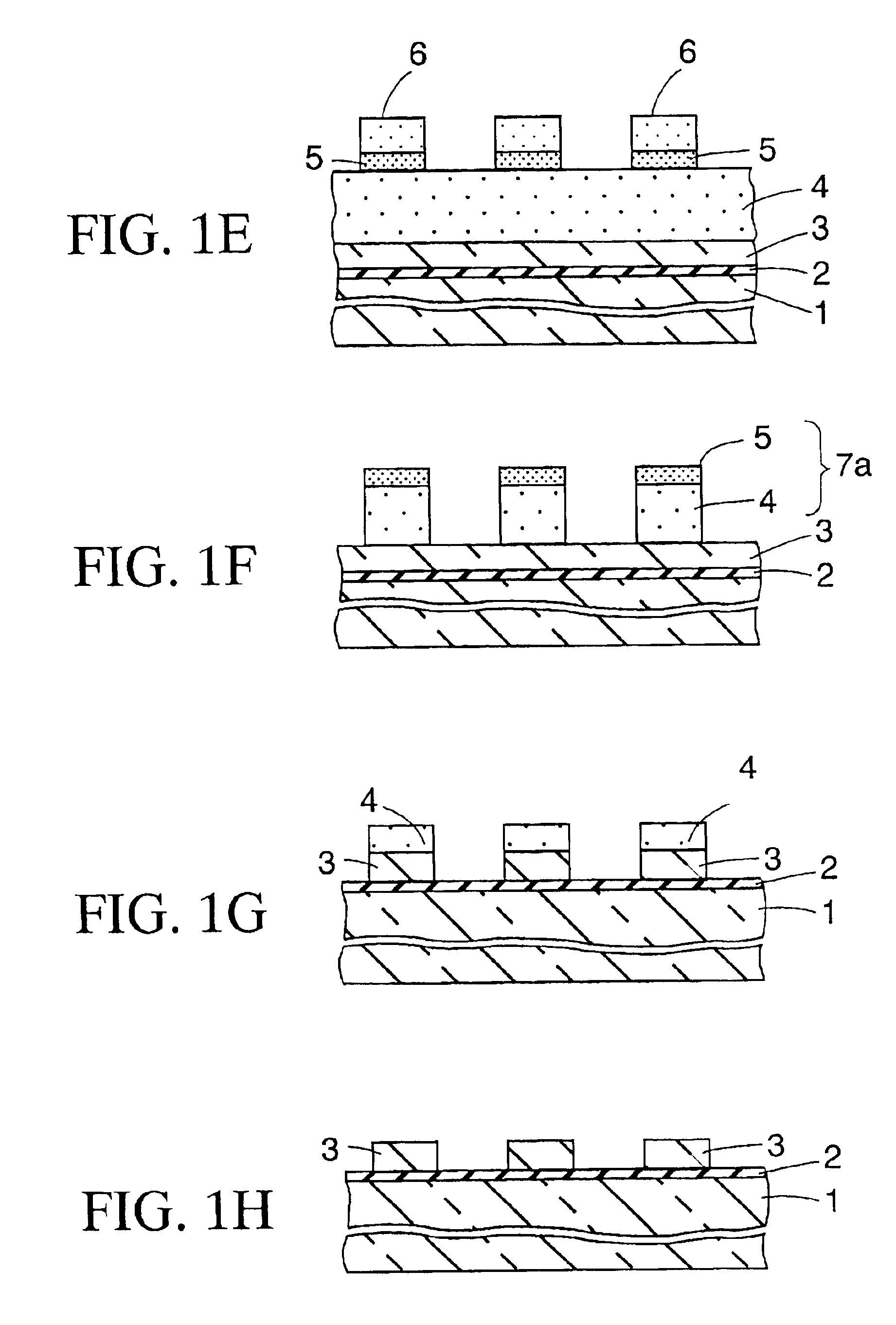
[0022]FIGS. 1A to 1H are sectional views showing film patterning steps according to an embodiment of the present invention.

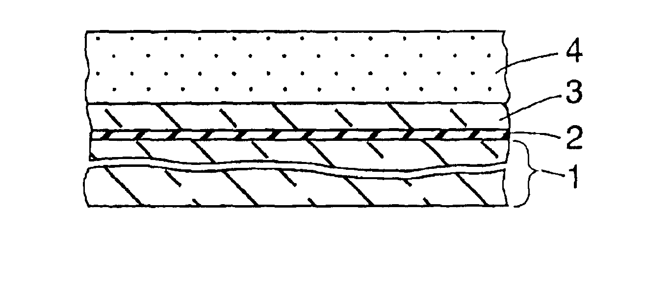
[0023]First, as shown in FIG. 1A, a polycrystalline or amorphous silicon film (patterning objective layer) 3 of 0.2 μm thickness is formed on a silicon substrate 1 via an insulating film 2 formed of silicon oxide, silicon nitride, or the like. Then, a lower resist layer 4 is formed on the silicon film 3 by the spin coating to have a thickness of 0.3 to 1.0 μm, for example, 0.5 μm. Then, the lower resist layer 4 is pre-baked at 150° C. for 60 seconds in the nitrogen atmosphere or the air and then post-baked at 300° C. for 60 seconds.

[0024]As the lower resist layer 4, the KrF resist material exposed by the KrF excimer laser, e.g., polyvinylphenol resin is employed. As the KrF resist material formed of the polyvinylphenol resin, there is...


PUM

PropertyMeasurementUnit
wavelengthaaaaaaaaaa

Abstract

There are provided steps of forming a lower resist layer on a patterning objective layer, forming an organic intermediate layer made of organic material, that contains no Si—O bond in its structure, on the lower resist layer, forming an upper resist layer made of alicyclic resin on the organic intermediate layer, forming a pattern by exposing / developing the upper resist layer, transferring the pattern of the upper resist layer onto the organic intermediate layer by etching the organic intermediate layer while using the upper resist layer as a mask, transferring a pattern of the organic intermediate layer onto the lower resist layer by etching the lower resist layer while using the organic intermediate layer as a mask, and etching the patterning objective layer while using the lower resist layer as a mask. Accordingly, a semiconductor device manufacturing method containing patterning steps employing a multi-layered resist structure, that is capable of suppressing deformation of the pattern of the upper resist layer formed of alicyclic compound, can be provided.

Description

CROSS-REFERENCE TO RELATED APPLICATION[0001]This application is based upon and claims priority of Japanese Patent Applications No. 2001-180584, filed in Jun. 14, 2001, the contents being incorporated herein by reference.BACKGROUND OF THE INVENTION[0002]1. Field of the Invention[0003]The present invention relates to a multi-layered resist structure and a manufacturing method of a semiconductor device and, more particularly, a multi-layered resist structure employed to pattern the film and a manufacturing method of a semiconductor device comprising the patterning steps employing such multi-layered resist structure.[0004]2. Description of the Prior Art[0005]In the fabrication of the semiconductor device, there are contained the step of forming recess portions by patterning the silicon substrate, the step of forming electrodes by patterning the silicon film, etc. Such patterning is carried out by etching partially the silicon substrate, the silicon film, etc. while using the resist patt...

Claims


Application Information

Patent Timeline
Patent Type & Authority Patents(United States)
IPC IPC(8): G03F7/11G03F7/075H01L21/027H01L21/308H01L21/311
CPCG03F7/0758G03F7/11H01L21/0275Y10S430/146H01L21/3086H01L21/31144H01L21/3081
Inventor OTOGURO, AKIHIKOTAKECHI, SATOSHI
Owner FUJITSU SEMICON LTD
Why Eureka
Try Eureka