Hybrid solid state/electrochemical photoelectrode for hydrogen production

a photoelectrode and solid-state technology, applied in the direction of energy input, sustainable manufacturing/processing, final product manufacturing, etc., can solve the problems of reduced corrosion protection at the oer catalyst layer, high optical loss of devices, and loss of catalytic activity

Inactive Publication Date: 2005-05-03
UNIV OF HAWAII
View PDF0 Cites 35 Cited by
  • Summary
  • Abstract
  • Description
  • Claims
  • Application Information

AI Technical Summary

Problems solved by technology

Such devices are prone to having high optical losses, loss of catalytic activity, and reduced corrosion protection at the OER catalyst layer.

Method used


Image

  • Hybrid solid state/electrochemical photoelectrode for hydrogen production
  • Hybrid solid state/electrochemical photoelectrode for hydrogen production
  • Hybrid solid state/electrochemical photoelectrode for hydrogen production

Examples


Embodiment Construction

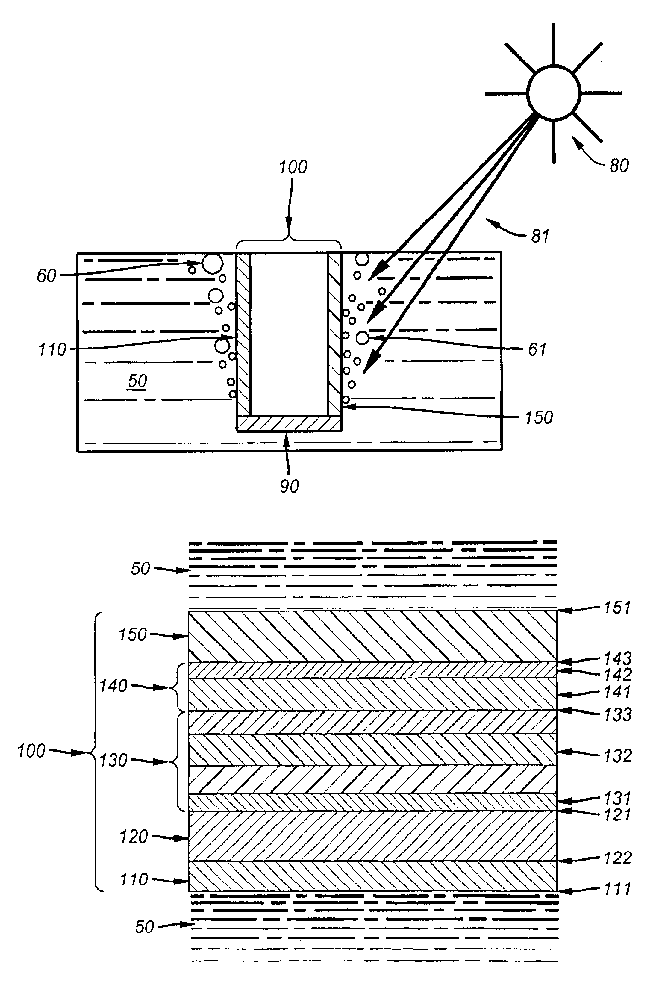
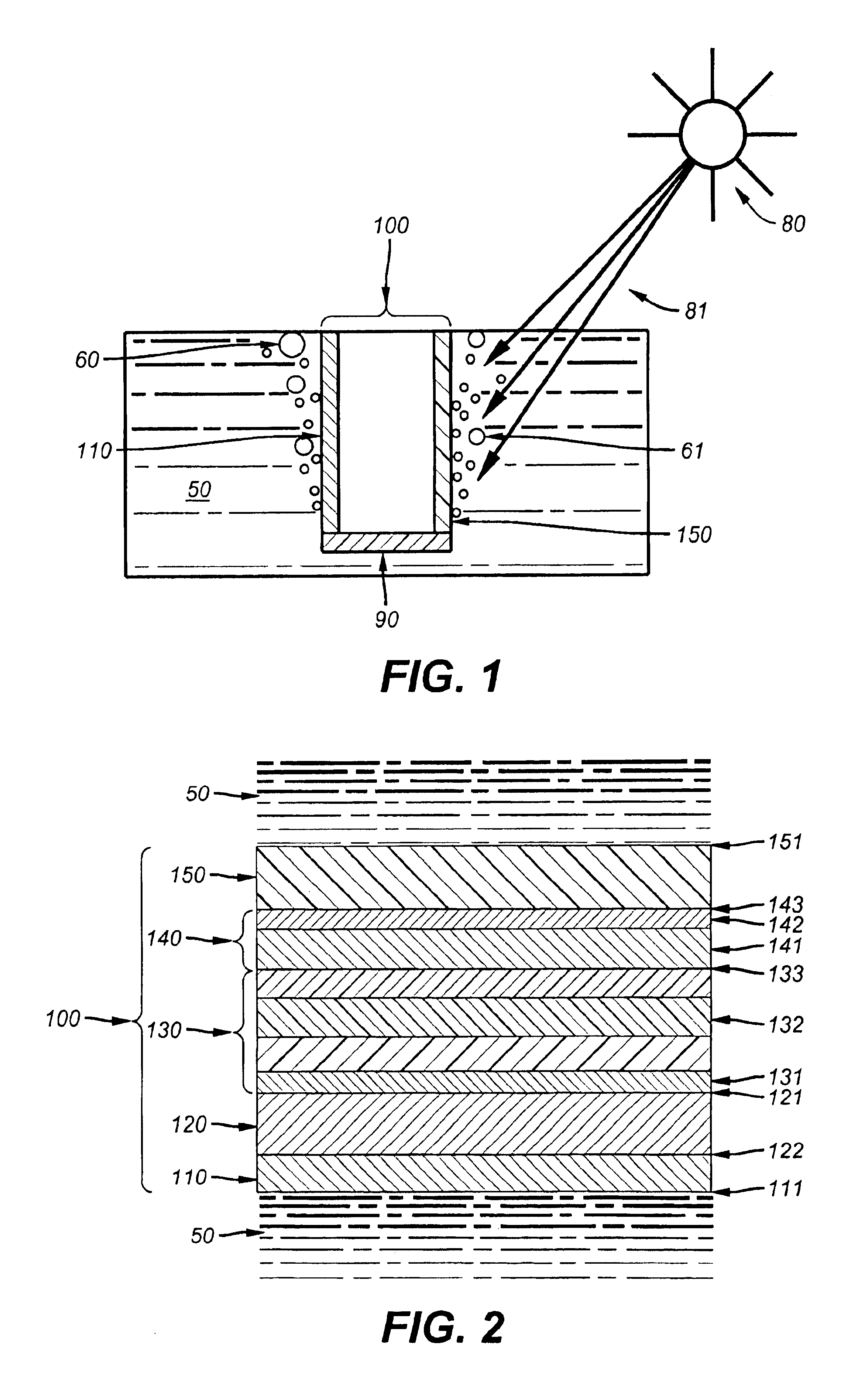
[0011]Referring now to FIG. 1, semiconductor device 100 is adapted to produce one or more gases 60 upon exposure to light 81, for example sunlight, when semiconductor device 100 is at least partially suspended in material 50 containing the constituent materials of gas 60. It is understood that, as used herein, “gas 60” may comprise a single gas, e.g. gas 60a, or a plurality of gases, e.g. gas 60a and / or gas 60b. Encapsulation film 90 may be deposited to protect one or more edges of semiconductor device 100 while semiconductor device 100 is suspended in material 50.

[0012]Referring now to FIG. 2, semiconductor device 100 comprises substrate 120, semiconductor layer 130 disposed on first surface 121 of substrate 120, photoactive semiconductor top layer 150, and interface layer 140 disposed between semiconductor layer 130 and photoactive semiconductor top layer 150. Photoactive semiconductor top layer 150 further comprises photoelectrochemical electrode junction 151 disposed at a surfac...


PUM

PropertyMeasurementUnit
wavelengthsaaaaaaaaaa
semiconductoraaaaaaaaaa

Abstract

The present invention relates to a semiconductor device for production of a gas from a material comprising the gas using light as the sole power source. In an embodiment, the semiconductor comprises a substrate; a solid-state semiconductor layer disposed on the substrate; a photoactive semiconductor top layer further comprising a photoelectrochemical electrode junction; and an interface layer disposed between the solid-state semiconductor layer and the photoactive semiconductor top layer. A surface of the photoactive semiconductor top layer is exposed to both a source of light such as the sun and to the material, e.g. a liquid electrolyte. The gas is liberated from the material, e.g. hydrogen liberated from a liquid electrolyte. It is emphasized that this abstract is provided to comply with the rules requiring an abstract which will allow a searcher or other reader to quickly ascertain the subject matter of the technical disclosure. It is submitted with the understanding that it will not be used to interpret or limit the scope or meaning of the claims.

Description

PRIORITY INFORMATION[0001]This application claims the benefit of U.S. Provisional Application No. 60 / 406,223 on Aug. 26, 2002.FIELD OF INVENTION[0002]The present invention relates generally to the field of design of semiconductor devices. More specifically, the present invention relates to semiconductor based gas generators such as may be used to produce hydrogen and / or oxygen using light as the sole power source.BACKGROUND OF THE INVENTION[0003]High efficiency photoelectrochemical (PEC) systems to produce hydrogen directly from water using sunlight as the energy source have been identified as a promising technology to meet long-term hydrogen-production goals at the United States Department of Energy.[0004]Photoactive devices with separate cathodes and anodes have been used in the art. Cathodes may include triple-junction amorphous silicon alloy (a-Si) type solar cell on a tin-oxide coated glass superstrate and may be physically separated from the anodes but electrically connected, ...

Claims


Application Information

Patent Timeline
Patent Type & Authority Patents(United States)
IPC IPC(8): C25B1/00H01G9/20
CPCC25B1/003H01G9/2027H01G9/205H01G9/2045Y02E10/542Y02P20/133Y02P70/50C25B1/55
Inventor MILLER, ERIC L.ROCHELEAU, RICHARD E.
Owner UNIV OF HAWAII
Why Eureka
Try Eureka