

Nonvolatile memory on SOI and compound semiconductor substrates and method of fabrication
a semiconductor substrate and non-volatile memory technology, applied in the direction of digital storage, diodes, instruments, etc., can solve the problem of undesirable forming of driver circuits in bulk monocrystalline silicon substrates
- Summary
- Abstract
- Description
- Claims
- Application Information
AI Technical Summary
Problems solved by technology
Method used
Image

Examples
first embodiment
[0021]In a first preferred aspect of the first embodiment, the SOI substrate includes a silicon layer 5 formed on an insulating layer 6, such as silicon oxide, silicon nitride, silicon oxynitride and / or other insulting layers. The insulating layer 6 is located on or over a bulk monocrystalline silicon substrate 7, as shown in FIG. 2A. Thus, the at least one driver circuit 2 is located in layer 5 above the bulk monocrystalline silicon substrate 7.
[0022]The SOI substrate (i.e., elements 5, 6, and 7) shown in FIG. 2A may be formed by the SIMOX (separation by implantation of oxygen) method. The SIMOX method includes providing a monocrystalline silicon substrate 7 and implanting oxygen below the surface of the substrate 7. The substrate 7 is then annealed to form a silicon oxide layer 6 in the substrate. Since the oxygen was implanted below the substrate 7 surface, a single crystal silicon layer 5 (which used to comprise the top section of the substrate 7) remains above the silicon oxide...
third embodiment
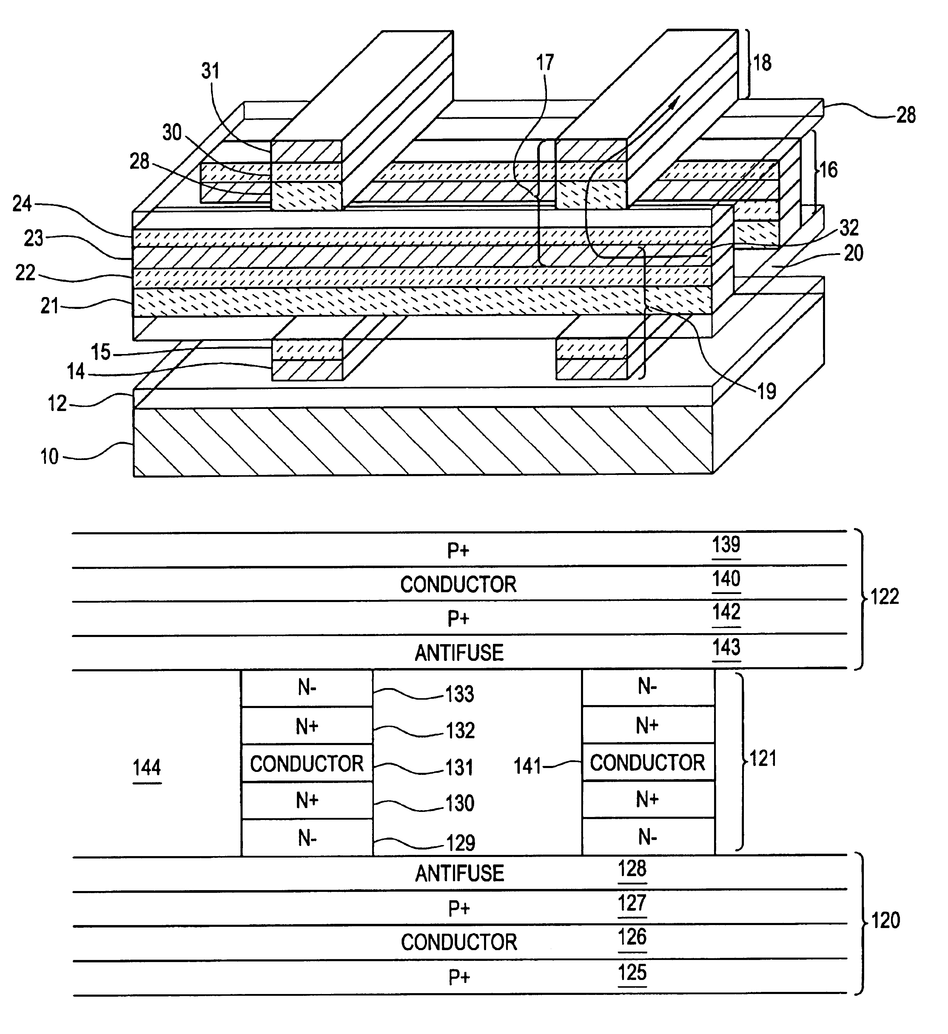
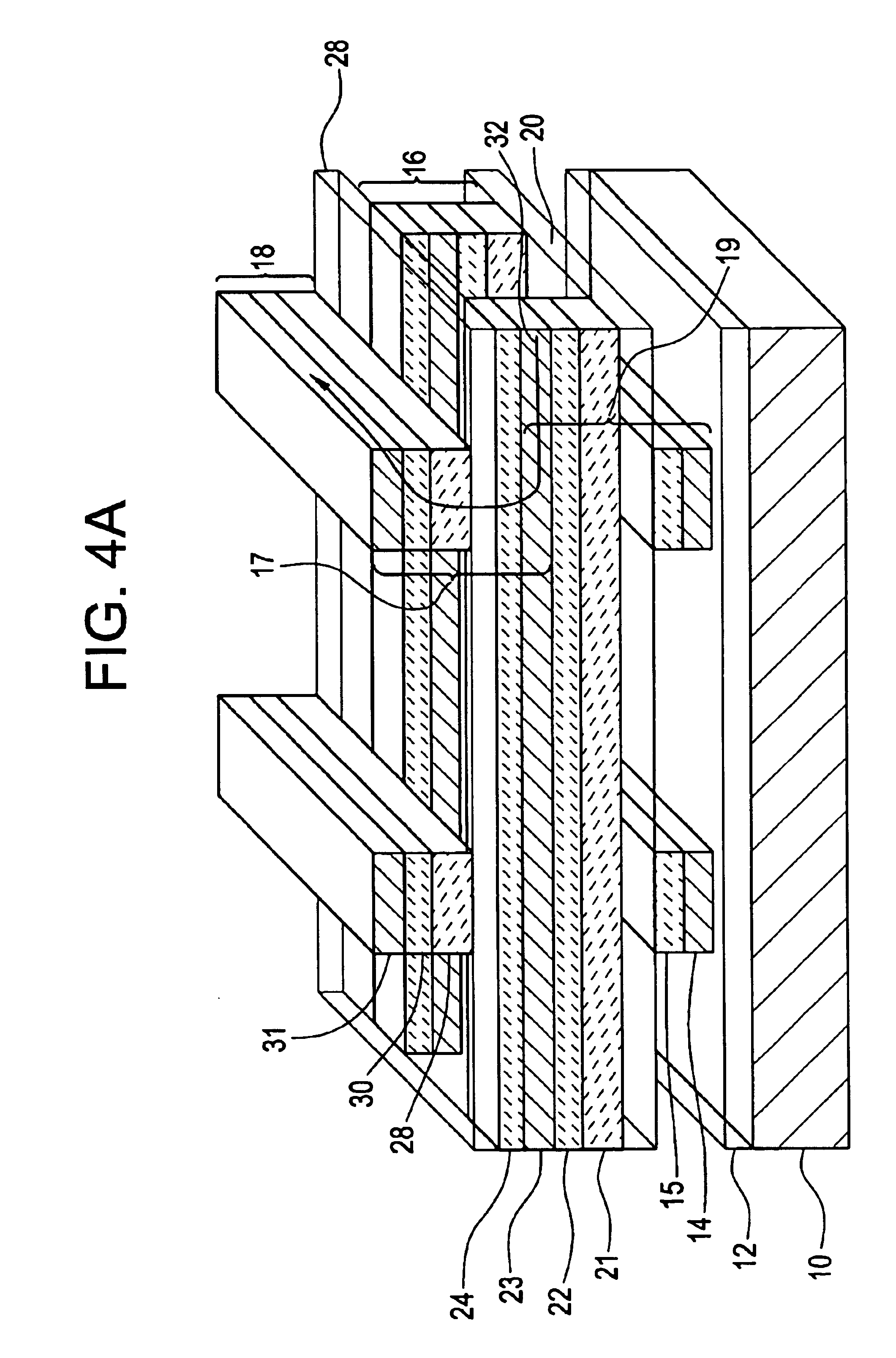
[0052]Some diode types may exhibit a higher leakage current than other diode types. Consequently, it may be desirable to form an array with only a single diode type. Specifically, the P− / N+ diodes have a higher leakage current than P+ / N− diodes. FIG. 4B illustrates an array of a preferred aspect of the third embodiment where, if the antifuse layer is breached, all the diodes will have a P+ / N− junction. Thus, there will be no diodes with a P− / N+ junction.
[0053]In FIG. 4B, three rail-stacks 120, 121, and 122 are illustrated which will create a P+ / N− diodes when an antifuse layer is breached. The first rail-stack 120 comprises a first P+ semiconductor (i.e., silicon) layer 125, a conductor 126, a second P+ layer 127 and an antifuse layer 128. The thickness of layers 125-127 may be 400 to 3000 Å, such as 1,000 / 500 / 1,000 Å, for layers 125, 126 and 127 respectively. The antifuse layer 128 may be about 20-40 Å, preferably about 30 Å thick.
[0054]The second rail-stack 121 comprises a first N...
ninth embodiment
[0095]The NMOS and PMOS transistors of the CMOS array may be formed adjacent to each other in the same device level in an alternating fashion (i.e., as alternating NMOS and PMOS transistors). However, in a preferred aspect of the present invention, the one charge carrier type transistors (i.e., NMOS or PMOS) are formed above the other charge carrier type transistors (i.e., PMOS or NMOS) with a common gate line (also known as a word line in memory devices) between them. Thus, the driver circuit 2 of the ninth preferred embodiment comprises a plurality of vertically stacked, common gate CMOS TFT transistors.
[0096]One device level of a vertically stacked, common gate CMOS array in a rail stack configuration according to the ninth preferred embodiment of the present invention is shown in FIG. 11. It should be noted that the array may also be arranged in a pillar or self-aligned TFT configurations illustrated in FIGS. 8 and 9. The CMOS array in FIG. 11 is similar to the array illustrated...
PUM
 Abstract
Description
Claims
Application Information