Scribe street width reduction by deep trench and shallow saw cut

a trench and trench cutting technology, applied in the field of semiconductor wafer dicing, can solve the problems of significant reliability risks, inability to safely reduce, and most significant limitation in reducing the distance between adjacent circuit chips, and achieve the effect of implementing

Inactive Publication Date: 2005-05-10
TEXAS INSTR INC
View PDF24 Cites 27 Cited by
  • Summary
  • Abstract
  • Description
  • Claims
  • Application Information

AI Technical Summary

Benefits of technology

[0009]It is a technical advantage of one or more embodiments of the invention that the embodiments can reach the goals of the invention with a low-cost manufacturing method without the cost of equipment changes and new capital investment, by using the installed fabrication equipment base, specifically the established wafer-fab etching techniques and automated sawing machines. Further, one or more embodiments of the invention can reach the goal of the invention without specific effort on aligning the etched trenches with the sawed streets, making the implementation of the invention in semiconductor manufacturing easy.
[0010]The technical advances represented by certain embodiments of the invention will become apparent from the following description of the preferred embodiments of the invention, when considered in conjunction with the accompanying drawings and the novel features set forth in the appended claims.

Problems solved by technology

For reasons of mechanical stability at high rotating speeds, the blades have to possess a particular thickness, which cannot safely be reduced.
In particular the third of these restrictions, namely the generation of cracks, creates the most significant limitation with respect to decreasing the distance between adjacent circuit chips.
In addition, those cracks represent significant reliability risks, since they tend to grow and widen under thermal and mechanical stress and thus eventually imperil the functionality of the integrated circuit.

Method used


Image

  • Scribe street width reduction by deep trench and shallow saw cut
  • Scribe street width reduction by deep trench and shallow saw cut
  • Scribe street width reduction by deep trench and shallow saw cut

Examples


Embodiment Construction

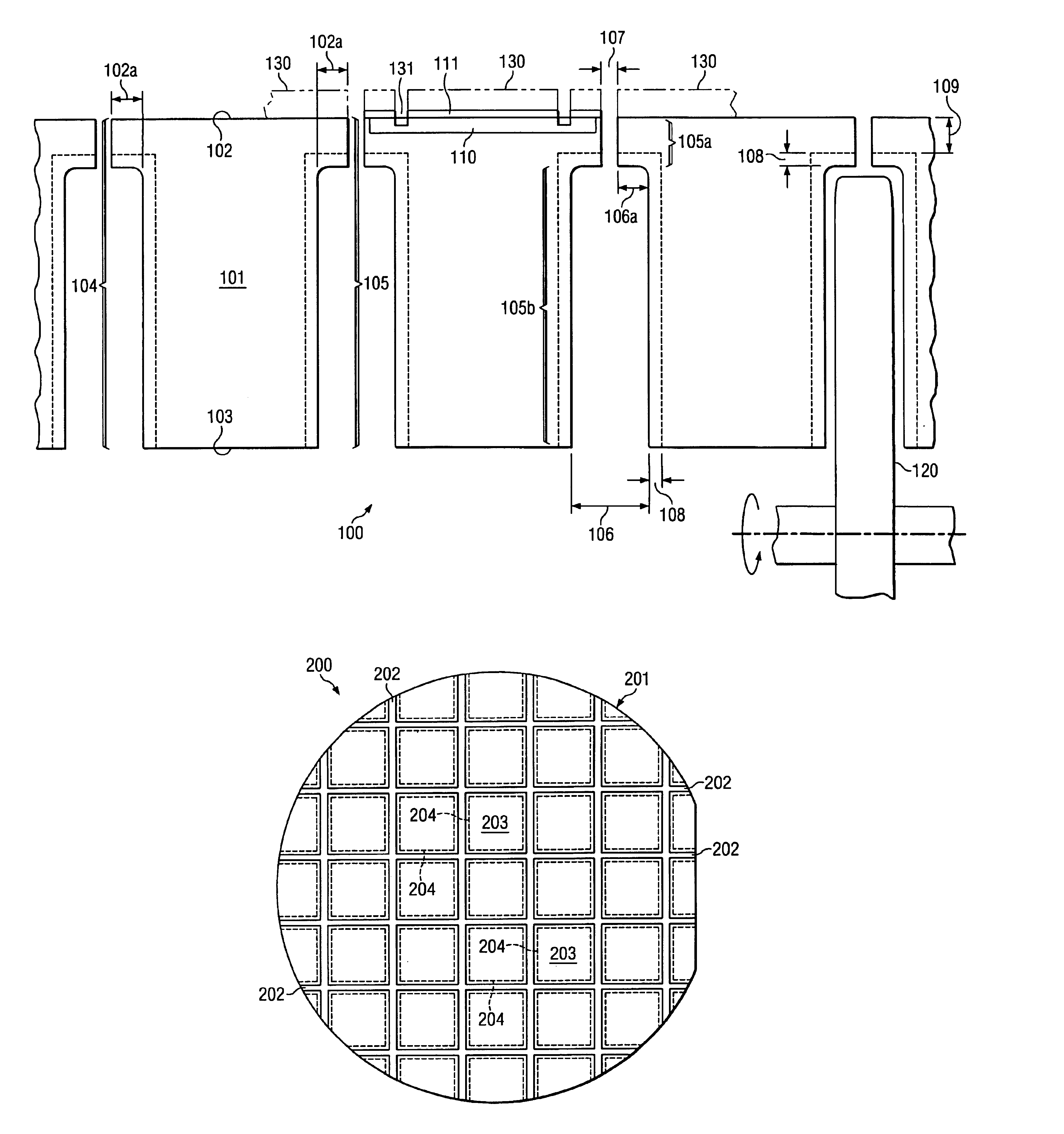
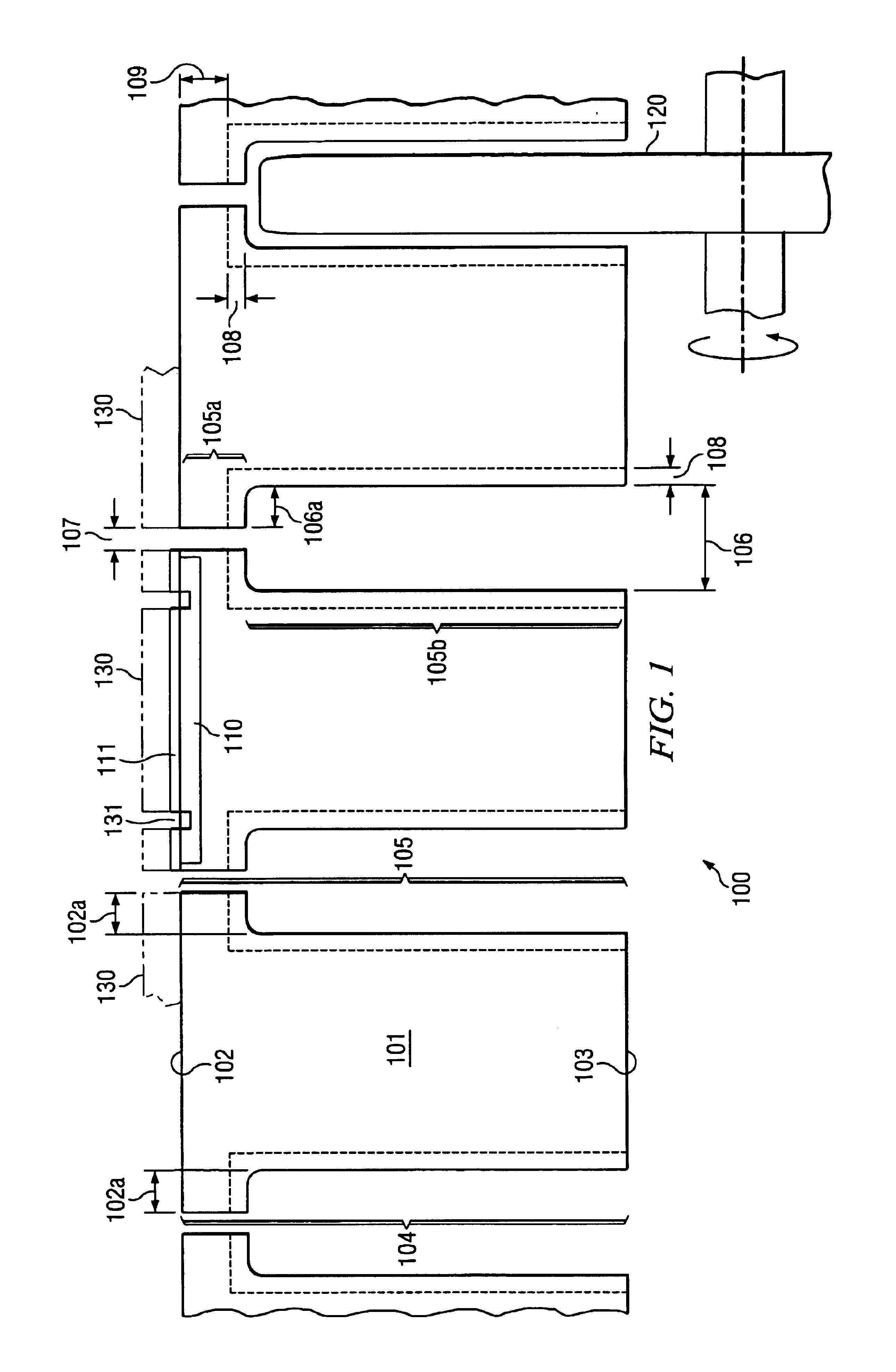
[0015]FIG. 1 illustrates schematically the cross section of a portion of a semiconductor wafer, generally designated 100, which has been singulated into a plurality of semiconductor chips 101. The vertical dimension of the wafer has been expanded in FIG. 1 for clarity. The semiconductor material of the wafer may be silicon, silicon germanium, germanium, gallium arsenide, aluminum gallium phosphide, indium phosphide, gallium phosphide, or any other semiconductor material used for fabricating semiconductor devices. Each chip 101 is in principle a cuboid, which has a top surface 102, a bottom surface 103, and four vertical side surfaces, of which only two surfaces 104 and 105 are indicated in FIG. 1. The top surface 102 includes the active electronic device 110, which may for some wafers include an integrated circuit, for other wafers a discreet device such as a diode, especially a light-emitting diode, or a controlled rectifier, or a power transistor. The bottom surface 103 is the pas...


PUM


Abstract

In a method to singulate a semiconductor wafer (100) into chips, trench streets (107) of predetermined depth (105a) are formed across the first, active wafer surface (102) to define the outline of the chips (101). Thereafter, the fabrication of the active first wafer surface is completed and protected. Then, the wafer is flipped to expose the second wafer surface (103), and the wafer is subjected to a cutting saw. The saw is aligned with the trenches in the first surface so that the saw cuts the second surface along streets (106), which extend the trenches through the wafer. The saw is stopped cutting at a depth (105b), when the saw streets just coalesce with the trench streets, respectively, whereby the chips are completely singulated.

Description

FIELD OF THE INVENTION[0001]The present invention is related in general to the field of semiconductor devices and more specifically to a method of dicing semiconductor wafers.DESCRIPTION OF THE RELATED ART[0002]With most semiconductor products, for example integrated circuits, transistors and diodes, a large number of elements are manufactured simultaneously on a large semiconductor wafer of silicon, gallium arsenide, gallium phosphide etc. The semiconductor industry employs the terms “singulation”, “dicing technologies” or “scribing technologies” to refer to those techniques for obtaining a large number of functional chips from each semiconductor wafer. Two dicing methods are particularly well known in the art: the grinding-cutting method, using a blade or wire saw, and the scribing method, using a diamond point. Modern silicon technology prefers the cutting method using high-speed rotating blades. For reasons of mechanical stability at high rotating speeds, the blades have to poss...

Claims


Application Information

Patent Timeline
Patent Type & Authority Patents(United States)
IPC IPC(8): H01L23/544H01L21/301H01L21/304H01L21/68H01L21/78
CPCH01L21/6836H01L21/78H01L21/3043H01L23/544H01L2924/0002H01L2221/68327H01L2924/00
Inventor HOWARD, GREGORY E.SWANSON, LELAND S.
Owner TEXAS INSTR INC
Why Eureka
Try Eureka