System and method for measuring characteristics of materials with the use of a composite sensor

Inactive Publication Date: 2005-05-10
MULTIMETRIXS
View PDF12 Cites 24 Cited by
  • Summary
  • Abstract
  • Description
  • Claims
  • Application Information

AI Technical Summary

Benefits of technology

[0018]It is an object of the present invention to provide a system, which is applicable to measurement of characteristics of conductive and non-conductive materials, e.g., of thin non-conductive and conductive films. It is another object of the invention to provide the aforementioned system, which is suitable for using the potentials of the resonance sensor technology to the extent unattainable with the known methods and systems. Another object is to provide the system for measuring thickness of thin dielectric films with high accuracy. Still another object is to provide the aforementioned system, which is suitable for measuring electrophysical surface characteristics of semiconductors.
[0019]The system of the invention for measuring characteristics of thin conductive and non-conductive material, such as bulk material or films, is based on the use of a resonance oscillating circuit that incorporates at least two components selected from the group consisting of an inductive coil and a capacitor, which in combination form a sensor that could be approached close to the surface to be measured. The measurement of the film or material characteristics, such as film resis

Problems solved by technology

However, the sensor disclosed in the aforementioned patent application could not completely solve the problems associated with accurate measurement of super-thin films, e.g., of those thinner than 500 Angstroms.
This is because the construction of the aforementioned sensor is limited with regard to the range of operation frequencies, i.e., the sensor cannot be used in frequencies exceeding several tens MHz.
Furthermore, the system which in this apparatus is used for stabilization of the distance between the sensor and the film is rather complicated, which makes the entire system complex and expensive.
But what is most important, the aforementioned complexity delays the system response in each measurement point, so that the system have low measurement efficiency and may not be suitable for used under mass production conditions.
The above problems restrict practical application of the method and apparatus of U.S. patent application Ser. No. 09/954,550 for measuring thickness of very thin films and deviations from the thickness in the aforementioned films.
Furthermore,

Method used


Image

  • System and method for measuring characteristics of materials with the use of a composite sensor
  • System and method for measuring characteristics of materials with the use of a composite sensor
  • System and method for measuring characteristics of materials with the use of a composite sensor

Examples


Embodiment Construction

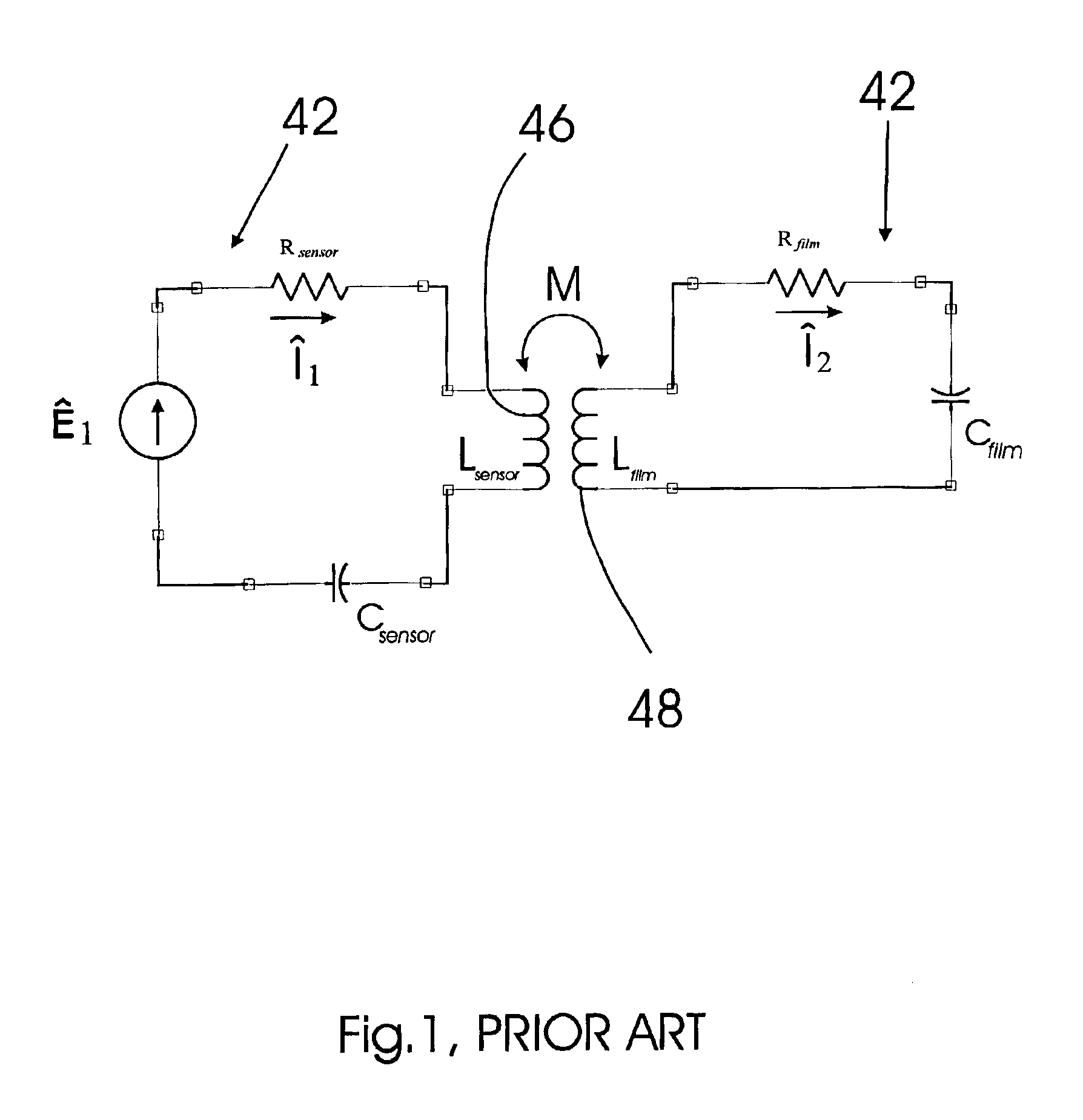
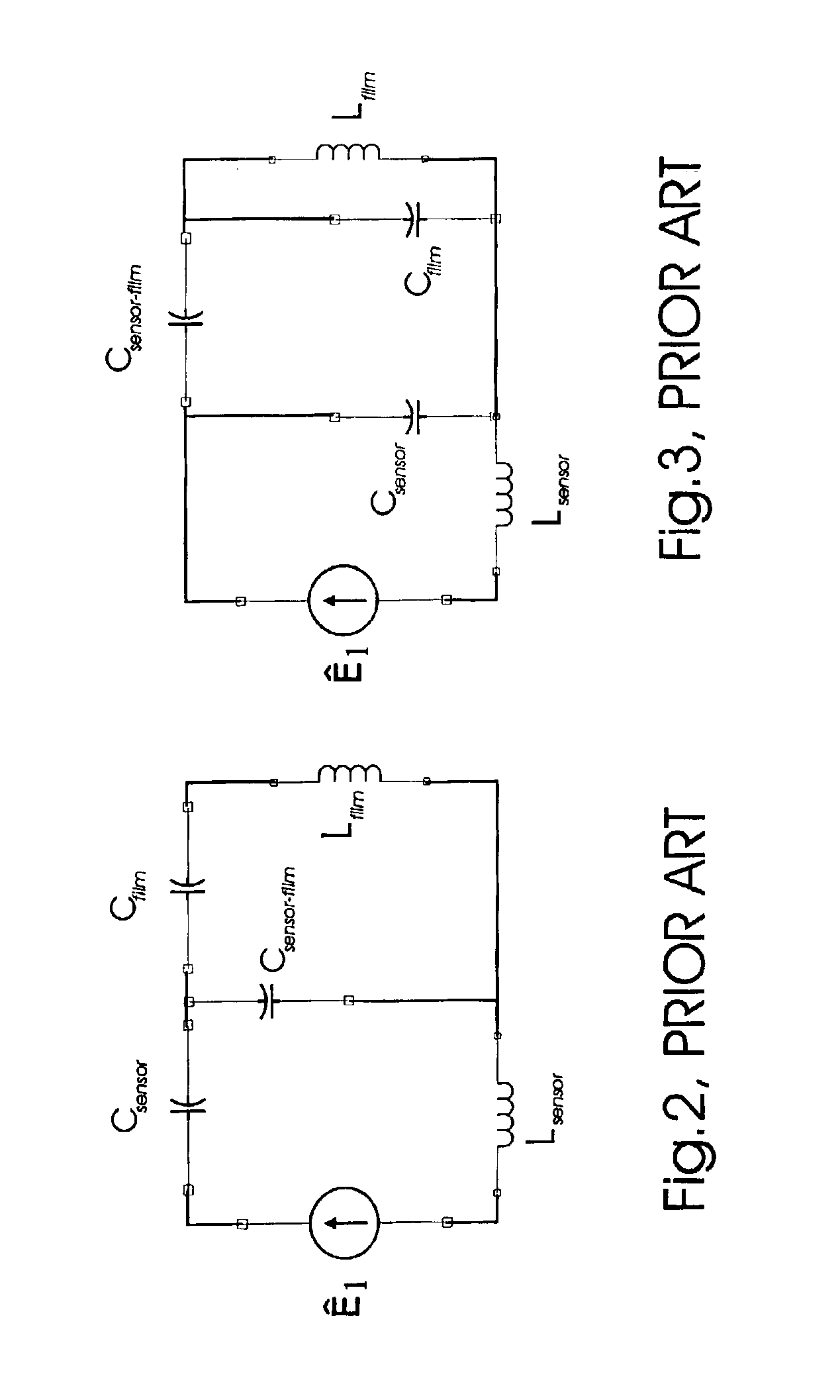
[0040]For better understanding of the inductive, capacitive, or inductive-capacitive coupling that is generated between the sensor of the invention and the virtual coil generated in the bulk material or in the film to be measured, it would be advantageous to refer to the description of the aforementioned U.S. patent application Ser. No. 434,625 filed by the same application in May 12, 2003. In that application, the equivalent “sensor-film” system was considered as a pair of two oscillation circuits having inductive-capacitive coupling. The first oscillating circuit comprised a closed-loop circuit that contained an inductance coil of the sensor per se, while the second oscillating circuit (i.e., the virtual oscillating circuit) was formed in the measured film and the aforementioned coupling comprised an inductive-capacitive interaction between the sensor and the film.

[0041]It is obvious that the sensor coil of the aforementioned coupled electric circuit generates an electromagnetic f...


PUM


Abstract

The system of the invention for measuring characteristics of thin conductive and non-conductive material, such as bulk material or films, is based on the use of a resonance oscillating circuit that incorporates at least two components selected from the group consisting of an inductive coil and a capacitor, which in combination form a sensor that could be approached close to the surface to be measured. The measurement of the film or material characteristics, such as film resistance (film thickness) or a dielectric constant (film thickness) of a non-conductive material, is based on the principle that the sensor is approached to the measured surface at a distance, at which the inductance and capacitance of the sensor generate in the measured material a virtual coil and an additional capacitance, which strongly depend on the characteristics of the measured material. As the sensor approached towards the surface to be measured, the sensor-material system generates a series of resonances having different values of power. One of these resonances can be defined as the so-called full resonance, which is characterized by the maximum value of the power, and hence provides the most accurate measurement and can be used for precisely determining the measurement distance. By comparing the results of measurements with those known from measuring the precalibrated films or materials under the same conditions, it becomes possible to determine the target characteristics of the films or materials.

Description

CROSS-REFERENCES TO RELATED APPLICATIONS[0001]The present patent application is related to the following earlier filed applications: U.S. patent application Ser. No. 954,550 filed on Sep. 17, 2001; U.S. patent application Ser. No. 359,378 filed by the same applicants as the present application on Feb. 7, 2003; U.S. patent application Ser. No. 386,648 filed by the same applicants as the present application on Mar. 13, 2003, and U.S. patent application Ser. No. 434,625 filed by the same applicants as the present application on May 12, 2003.FIELD OF THE INVENTION[0002]The present invention relates to the field of measurement of electrophysical characteristics of such materials as dielectrics, semiconductors, and metals, and more specifically, for measuring such characteristics as surface resistance, bulk resistance, dielectric constant, thickness of thin films, etc. In particular, the invention may find use in measuring characteristics of coating films on semiconductor wafers, hard dri...

Claims


Application Information

Patent Timeline
IPC IPC(8): G01B7/06G01B7/02G01R27/00G01R27/32G01R27/04G01R33/12
CPCG01B7/105
Inventor KESIL, BORISVELIKOV, LEONIDVOROBYEV, YURI
Owner MULTIMETRIXS
Why Eureka
Try Eureka