Metal mask structure and method for manufacturing thereof

Inactive Publication Date: 2005-05-17
SAMSUNG DISPLAY CO LTD
View PDF7 Cites 36 Cited by
  • Summary
  • Abstract
  • Description
  • Claims
  • Application Information

AI Technical Summary

Benefits of technology

[0012]Therefore, an object of the present invention is to provide a mask structure which can prevent a blur of the deposition pattern by minimizing the gap between the mask and the substrate being created by the welding flash, in case that the welding portion is contacted within a substrate to be deposited when the metal mask is welded to the frame.
[0013]As a result of devoting ourselves to solving the above described problems, the inventors has now found that a blur of a deposition pattern is virtually eliminated by forming a concave part in a welding portion between a metal mask and a frame and by securing and welding the metal mask and the frame within the concave part. This is because the height of a welding flash produced becomes lower and the flash barely protrudes from the surface of the mask to be contacted to the substrate, so that the substrate can intimately be contacted to the mask. Thus the present invention has been brought to completion. That is, the present invention relates to a metal mask s

Problems solved by technology

Also, a color conversion film or a color filter which requires to be patterned can be achieved by a conventional lithographic method, but there is a problem that a luminous efficiency decreases through the color conversion film or the color filter.
In particular, an organic dye used for the luminescent layer is poor in resistance to moisture or organic solvents, so that patterning through a wetting process which is a representative of the photolithographic method is difficult to be performed.
In addition, as for the electrodes which are formed on the organic luminescent layer, the organic dye is adversely affected by performing the pattern processing through the wetting process, so that in both cases, the dry process such as deposition is used and the patterning has been achieved by using a mask.
However, when a fine pattern is formed, a mask should be made thinner; otherwise the film thickness of a deposit around an opening becomes thinner, so that a deposit having an uniform thickness can not be obtained.
However, as the mask becomes thinner, the mask tends to be bent, so that a gap is formed between the mask and the substrate.
Therefore, especially at

Method used


Image

  • Metal mask structure and method for manufacturing thereof
  • Metal mask structure and method for manufacturing thereof
  • Metal mask structure and method for manufacturing thereof

Examples


Example

EXAMPLE 1

[0032]In this example, a mask for isolating an organic EL luminescent layer is described.

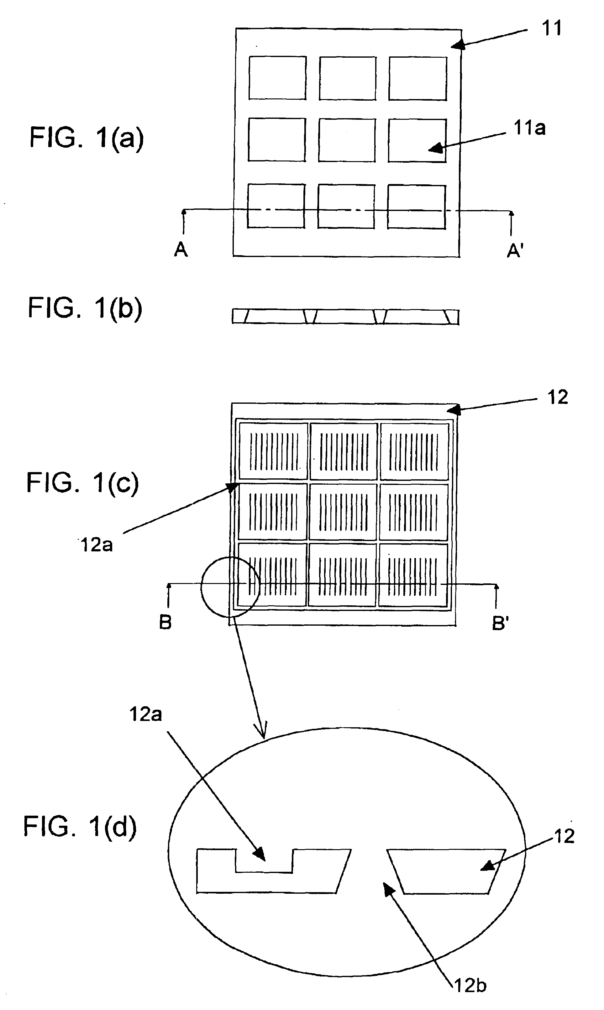
[0033]Firstly as shown in FIGS. 1(a) and 1(b), nine windows 11a for mask patterning, each of which has a size of 100×120 mm, were cut into a plate made of SUS 304 having a size of 400×400 mm and t=5 mm in order to obtain a metal mask frame 11, followed by performing mirror finish.

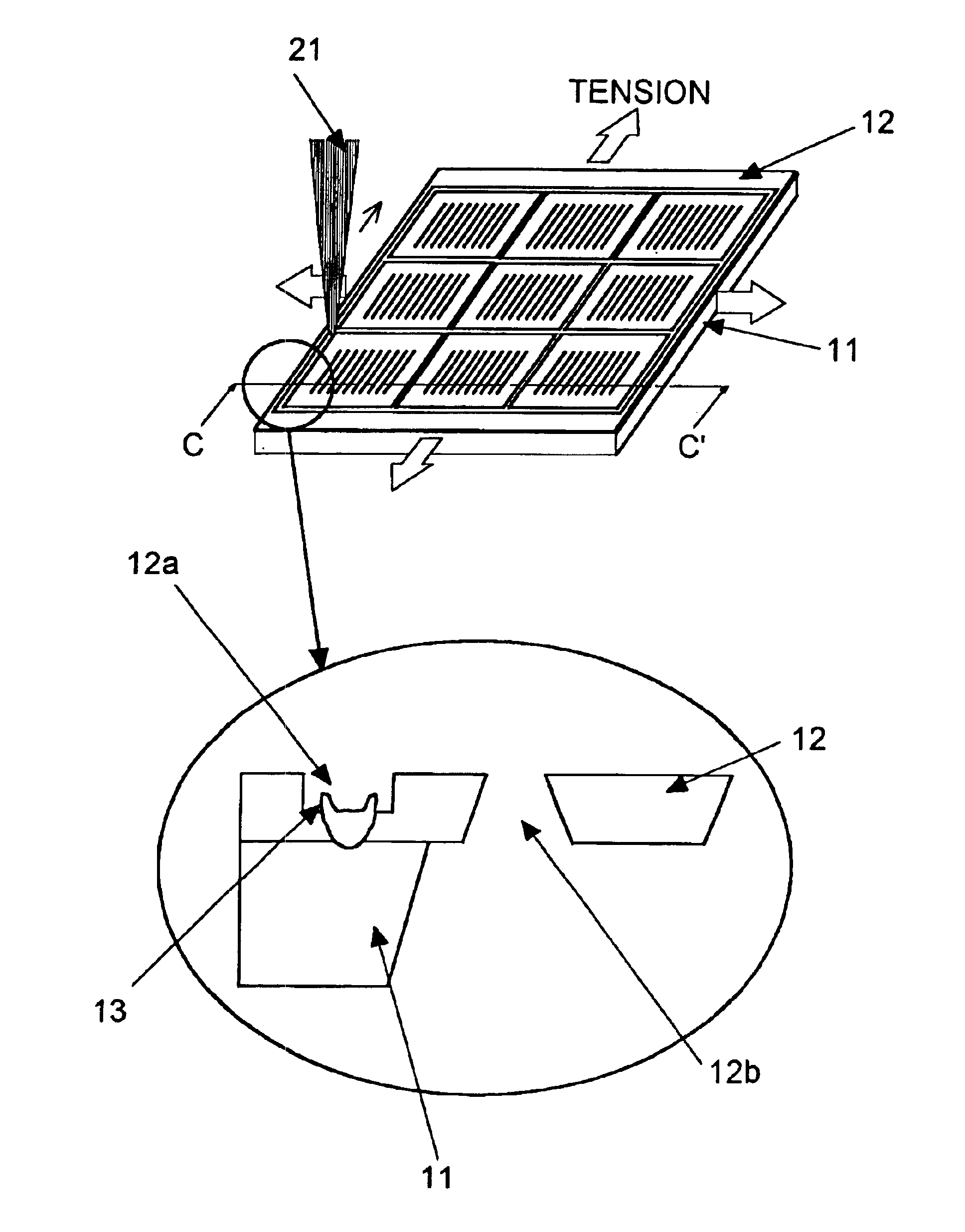
[0034]On the other hand, as shown in FIGS. 1(c) and 1(d), 320 slits 12b were patterned on a plate of SUS 304 having an outer size of 400×400 mm and t=100 μm by wet-etching in order to obtain a metal mask 12, in such a way that the slits with 360 μm pitches and with the slit width of 80 μm corresponded to the window portions of the above described frame. In addition, a concave part 12a at a welding portion was formed by cutting a surface which contacts a glass substrate in such a way that the cutting portion becomes a groove having a depth of 50 μm and a width of 1 mm.

[0035]In performing the welding, as shown in...

Example

EXAMPLE 2

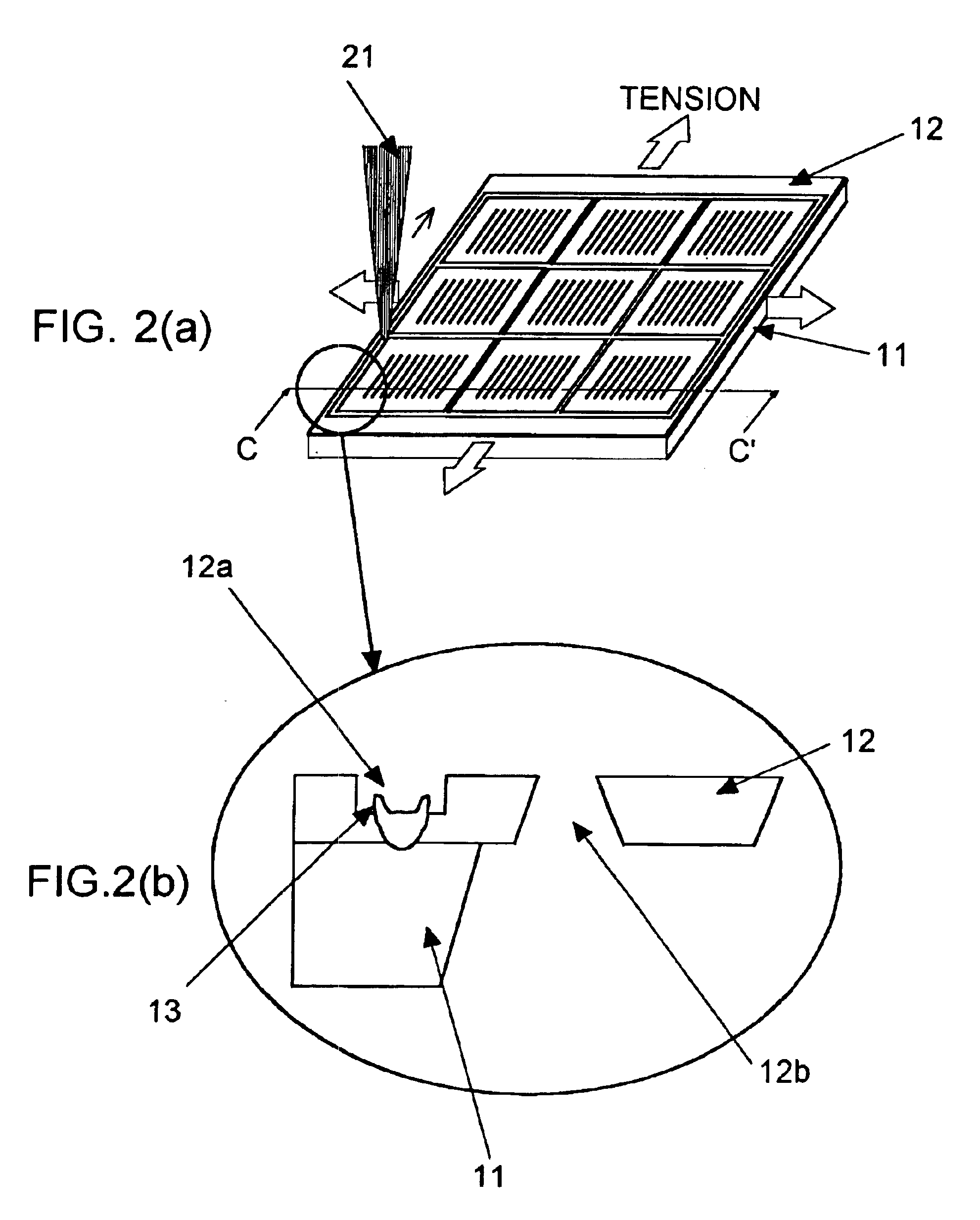
[0036]In this example, the manufacture of a metal mask for cathode isolation is described.

[0037]Nine windows for mask patterning each of which has a size of 120×100 mm were firstly cut into a plate of invar material (Fe65Ni35) having an outer size of 400×400 mm and t=5 mm in order to obtain a metal mask frame, followed by performing mirror finish.

[0038]On the other hand, 240 slits were patterned on a plate of SUS 304 having an outer size of 400×400 mm and t=100 μm by wet-etching in order to obtain a metal mask, in such a way that the slits with 360 μm pitches and with the slit width of 260 μm corresponded to the window portions of the above described frame. In addition, a concave part at a welding portion was formed by half-etching a surface which contacts a glass substrate, in such a way that the half-etching portion becomes a groove having a depth of 30 μm and a width of 0.8 mm.

[0039]In performing the welding, the metal mask is welded to the metal mask frame in such a way...

Example

[0045]A metal mask was welded to a frame as in the case of Example 1 or 2 except that a concave part was not provided to the welding portion. An EL device was formed by using this mask as in the case of the above described manufacturing example, but color mixture can be seen in the luminescent layers which were adjacent each other and a part of the cathode was shorted out.


PUM

PropertyMeasurementUnit
Depthaaaaaaaaaa
Shapeaaaaaaaaaa
Tensionaaaaaaaaaa

Abstract

A metal mask structure in which a metal mask 12 for depositing a thin layer is welded to a support frame 11 and the welding portion is placed within at least a substrate to be deposited, characterized in that a concave part 12a is formed on an opposite surface of a surface of said metal mask which is contacted to the frame, and the metal mask and the support frame are welded to each other within the concave part.

Description

BACKGROUND OF THE INVENTION[0001]1. Field of the Invention[0002]The present invention relates to a structure of a metal mask for depositing a deposit with the metal mask intimately held on a substrate and to a method for manufacturing thereof.[0003]2. Description of the Related Art[0004]In an organic electroluminescent device (an organic EL device) used for such as a display device or a flat panel display, electrons which are injected from a cathode and holes which are injected from an anode are recombined within an organic fluorescent dye interposed between both electrodes, in order to excite the dye for obtaining the luminescence. Therefore, this device attracts attention because this device has some excellent characteristics as compared with a liquid crystal display (LCD), that is, for example, an angle of visibility is large, a high contrast can be easily realized at the high brightness, miniaturization of the device can be achieved since a back light is not required due to the ...

Claims


Application Information

Patent Timeline
IPC IPC(8): B05C11/00B32B15/04B32B3/10H05B33/10C23C14/04C23C14/12C23C14/24H01L21/285H01L51/50H01L51/56H05B33/12
CPCB32B3/10B32B15/04C23C14/042C23C14/12Y10T428/24777Y10T428/24273Y10T428/24826Y10T428/24314H01L51/56H10K71/00C23C14/04
Inventor KITAZUME, EIICHI
Owner SAMSUNG DISPLAY CO LTD
Why Eureka
Try Eureka