Method for processing one-dimensional nano-materials

a nano-material and one-dimensional technology, applied in the field of one-dimensional nano-material processing, can solve the problems of carbon nanotubes formed by any of these methods alone that cannot satisfactorily be used as field emission materials, carbon nanotubes formed by arc discharge and laser vaporization methods have non-uniform heights and orientations, and are prone to being tangled together

Inactive Publication Date: 2005-05-17
TSINGHUA UNIV +1
View PDF3 Cites 21 Cited by
  • Summary
  • Abstract
  • Description
  • Claims
  • Application Information

AI Technical Summary

Benefits of technology

[0010]In view of the above-described drawbacks, an object of the present invention is to provide a method for processing one-dimensional nano-materials which reduces shielding between adjacent one-dimensional nano-materials.
[0013]In order to achieve the objects set out above, a preferred method of the present invention for processing one-dimensional nano-materials comprises the following steps: providing a substrate; forming one-dimensional nano-materials on the substrate, the one-dimensional nano-materials being substantially parallel to each other and each being substantially perpendicular to the substrate, the one-dimensional nano-materials cooperatively defining a top surface distal from the substrate; and applying physical energy by means of a high-energy pulse laser beam to the top surface of the one-dimensional nano-materials. The resulting one-dimensional nano-materials have sharp, tapered tips. Distances between adjacent tips are approximately uniform, and are relatively large. This reduces shielding between adjacent one-dimensional nano-materials. The tips also contribute to a decreased threshold voltage required for field emission by the one-dimensional nano-materials.

Problems solved by technology

Carbon nanotubes formed by any of these methods alone cannot satisfactorily be used as field emission material for the following reasons.
Carbon nanotubes formed using the arc discharge and laser vaporization methods have non-uniform heights and orientations, and are prone to be tangled together.
If the carbon nanotubes are directly used as field emission material, they tend to reduce field concentration and field efficiency.
In addition, cavities at the tips of carbon nanotubes are encapsulated by catalytic metal particles, thereby reducing field concentration and efficiency.
This makes the method unduly time-consuming.
This induces shielding between adjacent carbon nanotubes, reduces field concentration and efficiency, and increases a threshold voltage of field emission.
Other one-dimensional nano-materials such as nanowires, nanorods and nanofibers that are used as field emission materials have similar problems and limitations as those described above in relation to carbon nanotubes.
These difficulties greatly limit industrial applications of the one-dimensional nano-materials.

Method used


Image

  • Method for processing one-dimensional nano-materials
  • Method for processing one-dimensional nano-materials
  • Method for processing one-dimensional nano-materials

Examples


Embodiment Construction

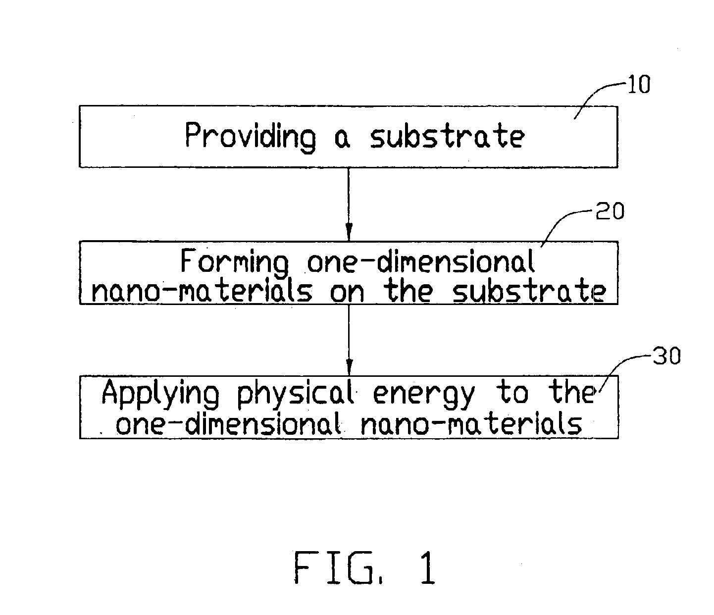
[0025]A preferred method for processing one-dimensional nano-materials according to the present invention will be described with reference to the flowchart of FIG. 1.

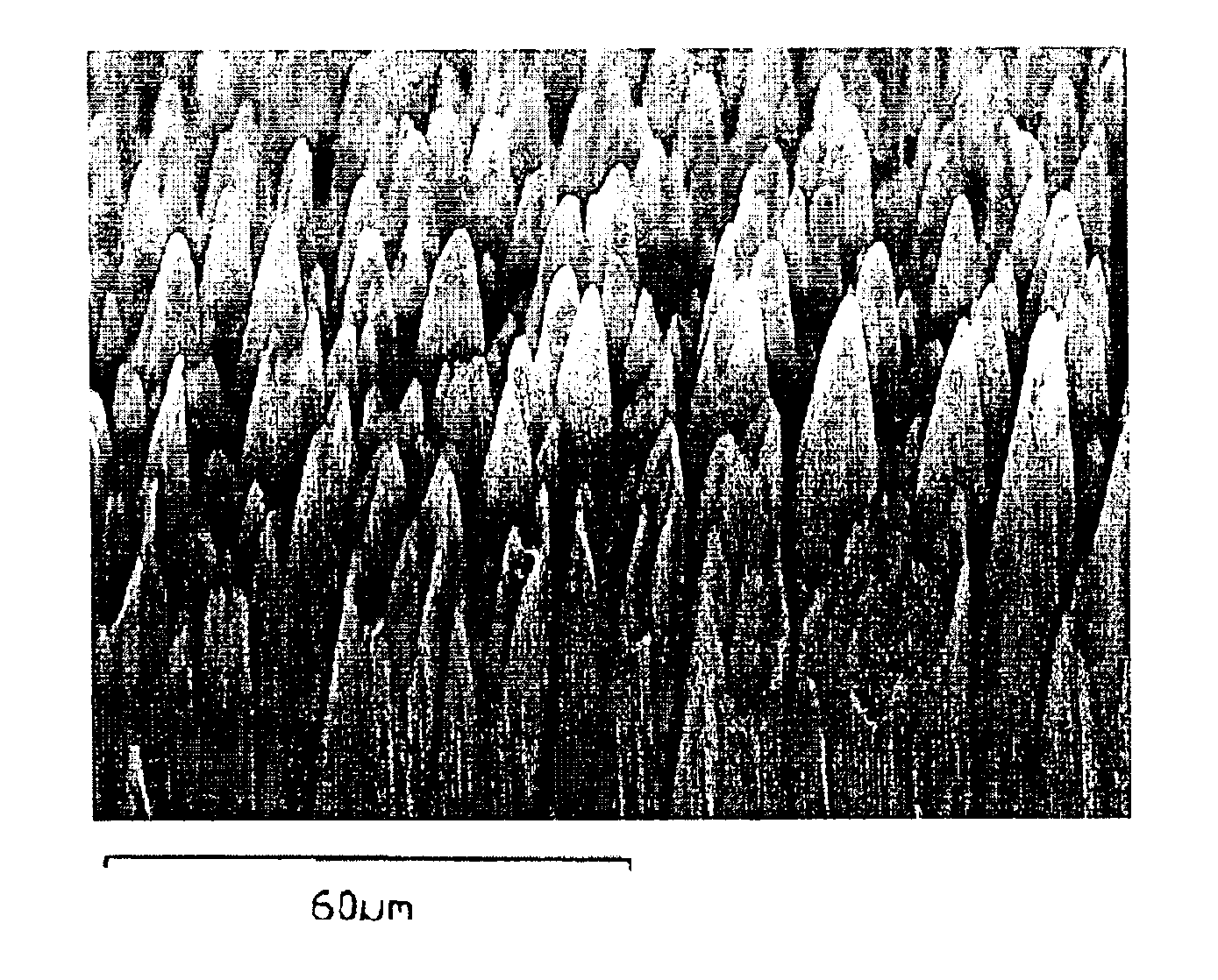
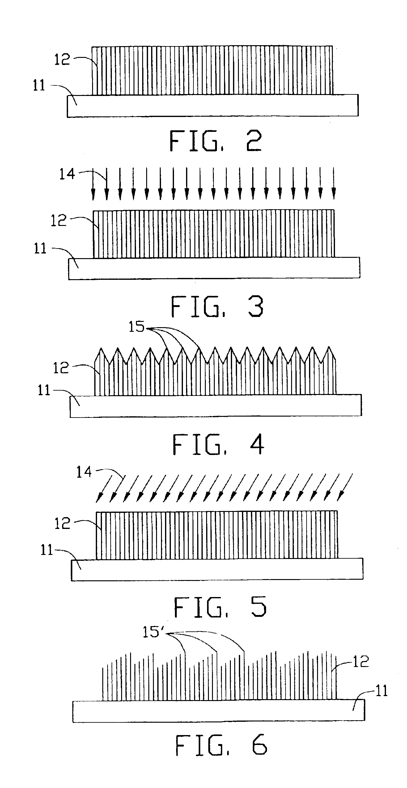
[0026]Referring also to FIG. 2, a substrate 11 is first provided (step 10). The substrate 11 can be made of glass, silicon, alumina or another suitable material. Then one-dimensional nano-materials 12 are formed on the substrate 11 (step 20). The one-dimensional nano-materials 12 can be carbon nanotubes, nanofibers, nanorods, or nanowires. In the preferred method, the one-dimensional nano-materials 12 are carbon nanotubes 12. The carbon nanotubes 12 can be formed by growing them on the substrate 11 directly, or by transplanting pre-prepared carbon nanotubes onto the substrate 11. The carbon nanotubes 12 are substantially parallel to each other, and are each substantially perpendicular to the substrate 11. The carbon nanotubes 12 cooperatively define a top surface (not labeled) distal from the substrate 11.

[0027]Referrin...


PUM

PropertyMeasurementUnit
wavelengthaaaaaaaaaa
areaaaaaaaaaaa
angleaaaaaaaaaa

Abstract

A method for processing one-dimensional nano-materials includes the following steps: providing a substrate (11); forming one-dimensional nano-materials (12) on the substrate, the one-dimensional nano-materials being substantially parallel to each other and each being substantially perpendicular to the substrate, the one-dimensional nano-materials cooperatively defining a top surface distal from the substrate; and applying physical energy (14) by means of a high-energy pulse laser beam to the top surface of the one-dimensional nano-materials. The resulting one-dimensional nano-materials have sharp, tapered tips (15, 15′). Distances between adjacent tips are approximately uniform, and are relatively large. This reduces shielding between adjacent one-dimensional nano-materials. The tips also contribute to a decreased threshold voltage required for field emission by the one-dimensional nano-materials.

Description

BACKGROUND OF THE INVENTION[0001]1. Field of the Invention[0002]The present invention relates to methods for processing nano-materials, and more particularly to methods for processing one-dimensional nano-materials. This application relates to a contemporaneously filed application having the same applicant and same assignee with the instant invention, and titled “FIELD EMISSION DEVICE” referring to the same device.[0003]2. Description of Prior Art[0004]Nano-materials are materials having special electrical, magnetic, optical, thermal, physical and chemical properties. Nano-materials play an important role in research in mesoscopic science and in nano-devices. One-dimensional nano-materials are those whose structure have an aspect ratio in the range from 10 to 1000. Carbon nanotubes are a well-known kind of one-dimensional nano-material.[0005]Carbon nanotubes have superior electron emission capability at low emission voltages, generally less than 100 volts. Furthermore, carbon nanotu...

Claims


Application Information

Patent Timeline
Patent Type & Authority Patents(United States)
IPC IPC(8): C30B29/60C30B33/00C30B33/04C30B29/00H01J9/02B82B3/00C01B31/02
CPCB82Y10/00B82Y30/00C30B29/605H01J9/025C30B33/04Y10S977/901H01J2201/30469
Inventor LIU, LIANGFAN, SHOUSHAN
Owner TSINGHUA UNIV
Why Eureka
Try Eureka