Supercharge Your Innovation With Domain-Expert AI Agents!

Process integration for integrated circuits

a technology of integrated circuits and integrated circuits, applied in the direction of basic electric elements, electrical apparatus, semiconductor devices, etc., can solve the problems of insufficient active area corner rounding of support devices, performance degradation of support devices, and different circuit requirements of memory cells and support circuitry

Inactive Publication Date: 2005-05-17
INFINEON TECH AG
View PDF5 Cites 3 Cited by
  • Summary
  • Abstract
  • Description
  • Claims
  • Application Information

AI Technical Summary

Benefits of technology

The patent describes a process for making integrated circuits with corner rounding. A support region is created on a substrate with trench isolations, and an active area is formed between the trench isolations. Etch stop layers are deposited on the substrate and remove a portion of the first etch stop layer to expose edge portions of the active area. The second etch stop layer is then removed, and the edge portions of the active area are oxidized. The technical effect of this process is to create a more precise and uniform corner rounding in the integrated circuit, which improves its performance and reliability.

Problems solved by technology

Unfortunately, circuit requirements for the memory cells and support circuitry are different.
For example, current integration processes for vertical array memory cells result in an insufficient active area corner rounding for support devices.
This can undesirably lead to performance degradation for support devices.

Method used


Image

  • Process integration for integrated circuits
  • Process integration for integrated circuits
  • Process integration for integrated circuits

Examples


Embodiment Construction

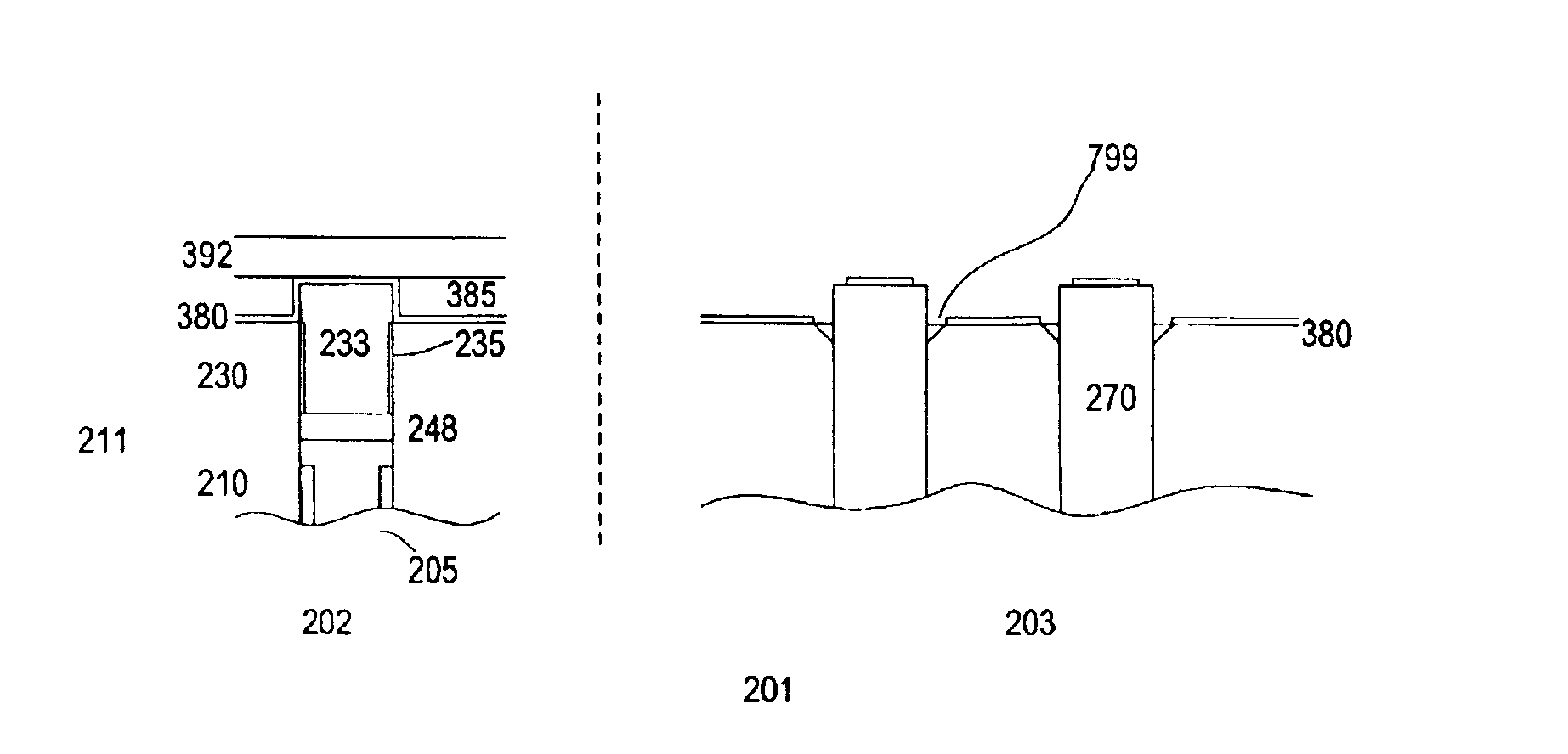
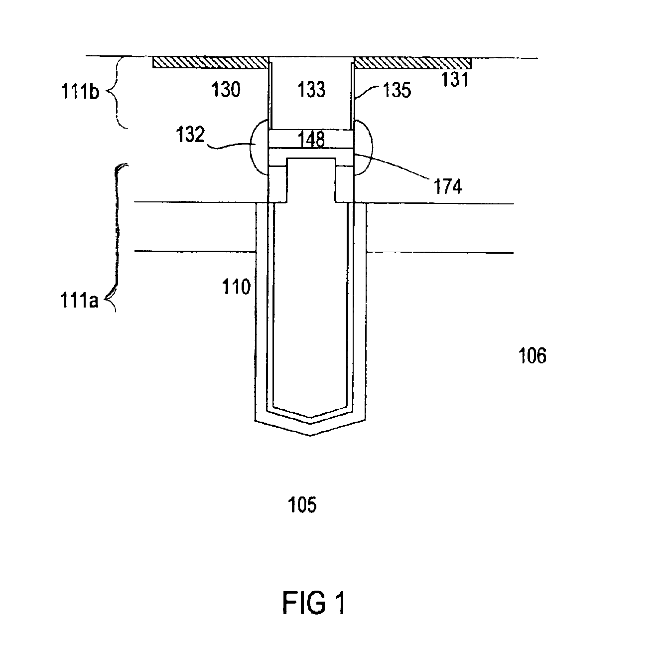
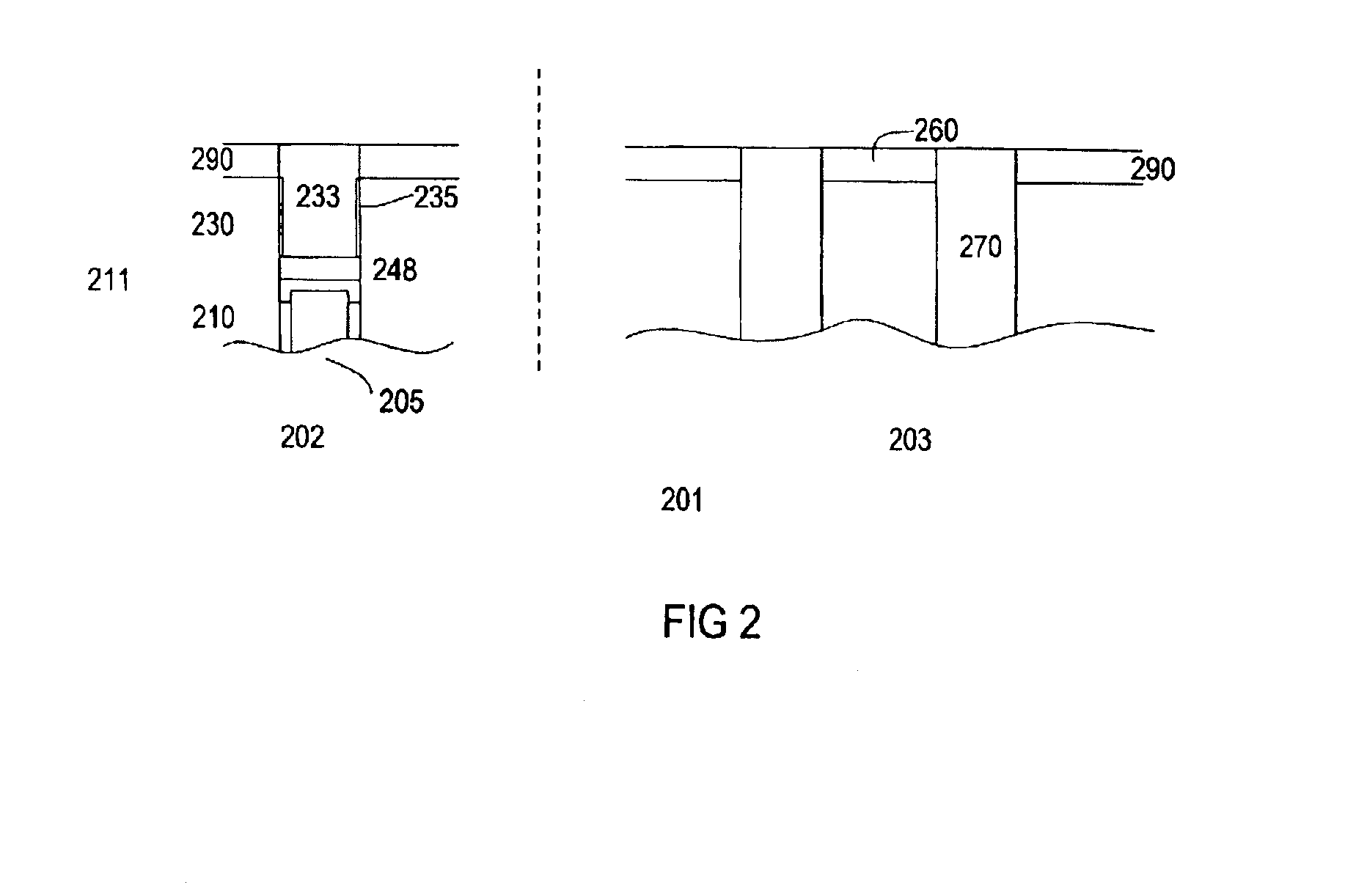
[0008]The invention relates to the fabrication of ICs with memory cells. The ICs, for example, are memory ICs. Other types of ICs, such as system on chip, are also useful. In one embodiment, the invention relates to the fabrication of memory cells having a trench capacitor coupled to a vertical transistor. Preferably, the memory cells are formed without compromising performance by sacrificing the needs of support devices. More preferably, the active areas in the support region are provided with sufficient corner rounding.

[0009]Typically, in IC fabrication, a plurality of ICs are formed on the wafer in parallel. After processing is finished, the wafer is diced to separate the ICs into individual chips. The chips are then packaged, resulting in a final product that is used in, for example, consumer products such as computer systems, cellular phones, digital cameras, personal digital assistants (PDAs), and other products.

[0010]FIGS. 2-8 show a process for forming an IC in accordance wi...


PUM


Abstract

A process for fabricating integrated circuits is disclosed. In particular, the process includes rounding corners of the active regions. In one embodiment, a substrate prepared with a support region having an active area between first and second trench isolations. The top surfaces of the trench isolations extend above the surface of the substrate. First and second etch stop layers are deposited on the substrate, lining the substrate surface and trench isolations without filling the gap. The etch stop layers can be etched selective to each other and layers beneath and or above. The second etch stop layer includes horizontal and vertical portions. An etch selectively removes the vertical portions of the etch stop layer. An isotropic etch is then performed, removing exposed portions of the first etch stop layer. The second etch stop layer acts as an etch mask. The etch also creates an undercut beneath the second etch stop layer, exposing edge portions of the active area. The second etch stop layer is removed, following by oxidizing the edge portions of the active area unprotected by the first etch stop layer.

Description

BACKGROUND OF INVENTION[0001]An integrated circuit can have millions of circuit features, such as transistors and capacitors, formed on a chip. Some ICs include an array of memory cells for storing information. To access the memory cells, addressing circuitry such as decoders, drivers and sense amplifiers (generally referred to as support circuitry) are provided. The chip is separated into array and support regions in which memory cells and support circuitry are respectively located. One type of memory cell 105 includes a trench capacitor coupled to a vertical transistor 130, as shown in FIG. 1. Such types of memory cells are described in, for example, Weis et. al., “A Highly Cost Efficient 8F2 DRAM Cell with a Double Gate Vertical Transistor Device for 100 nm and Beyond”, International Electron Device Meeting IEDM, Washington (2001), which is herein incorporated by reference for all purposes. The capacitor is formed in a lower portion 111a of a trench created in a substrate 106. Th...

Claims


Application Information

Patent Timeline
Patent Type & Authority Patents(United States)
IPC IPC(8): H01L21/02H01L21/76H01L21/70H01L21/8242H01L21/311H01L21/8238H01L29/94H10B12/00
CPCH01L29/945H01L27/10864H01L27/10894H10B12/0383H10B12/09
Inventor BEINTNER, JOCHEN
Owner INFINEON TECH AG
Features
  • R&D
  • Intellectual Property
  • Life Sciences
  • Materials
  • Tech Scout
  • Unparalleled Data Quality
  • Higher Quality Content
  • 60% Fewer Hallucinations
Learn More