[0008]In circuit boards with integrated grounding, PCB mounting holes provide a mesh location for the
system grounds. As described, conventional multi-layer circuit boards utilize
printed circuit board (PCB) mounting holes as the mesh points for the
system grounds. During operation of the circuit board components create a
potential difference between two adjacent PCB mounting holes in the circuit board and induce a current flow between the PCB mounting holes. As the
operating frequency of circuit board components or
electronics increases, however, to reduce the amount of current induced between PCB mounting holes on the circuit board, the distance between meshing points decreases. The use of conventional circuit having PCB mounting holes located at relatively large distances from each other (e.g., 12″×14″ circuit boards having nine PCB mounting holes) with circuit board components having a relatively high
operating frequency, therefore, allows induction of current flow between the PCB mounting holes and generation of EMI
radiation that can interfere with operation of the circuit board.
[0009]For a circuit board having components operating at a relatively
high frequency, a manufacturer can minimize the induction of current between adjacent PCB mounting holes by increasing the number of PCB mounting holes within the circuit board. However, conventional PCB mounting holes have a
diameter of approximately 9.5 mm. Increasing the number of PCB mounting holes in a circuit board reduces the amount of real estate on the circuit board available for circuit board components and traces.
[0010]Also as described above, conventional fasteners and minimally compliant stand-offs generate a stress on the surface of the circuit board after attachment to the PCB mounting holes. The stress, in turn, can fracture or cause failure of circuit board component ball grid arrays (BGA) positioned relatively close to the PCB mounting holes. As a result, the PCB mounting holes require that BGA devices mount to the circuit board at a 0.5 inch
radius from the center of each PCB mounting hole to minimize stress on the BGA. Increasing the number of PCB mounting holes in a circuit board, therefore, reduces the amount of real estate on the circuit board available for BGA mounted circuit board components. Furthermore, the stress generated by the conventional fasteners and minimally compliant stand-offs on the circuit board causes the conductive layers (e.g., both grounding and
signal carrying layers) to contact each other through the non-conductive layers. Such contact short circuits the signals carried by the layers and, in turn, causes the circuit board to malfunction.
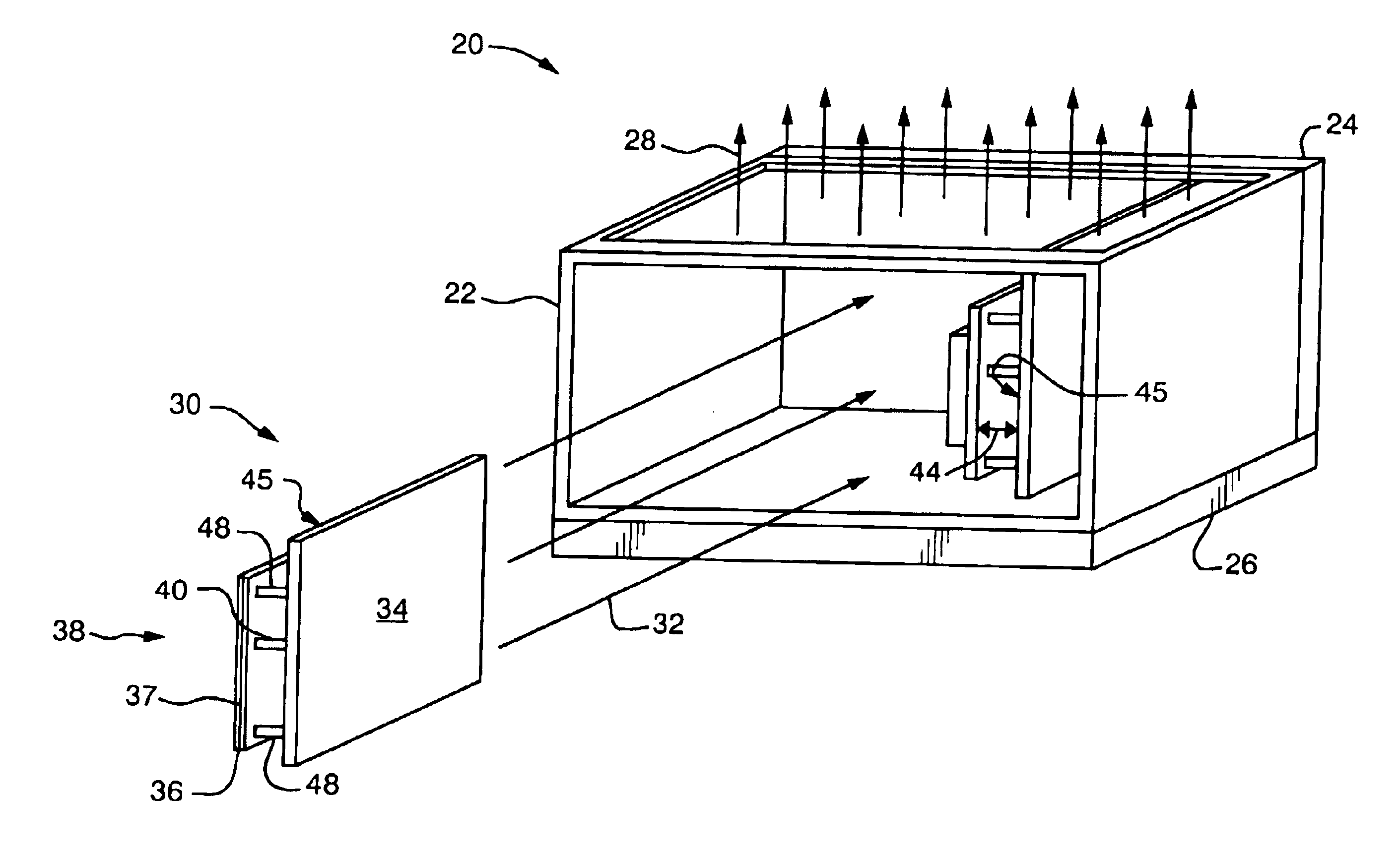
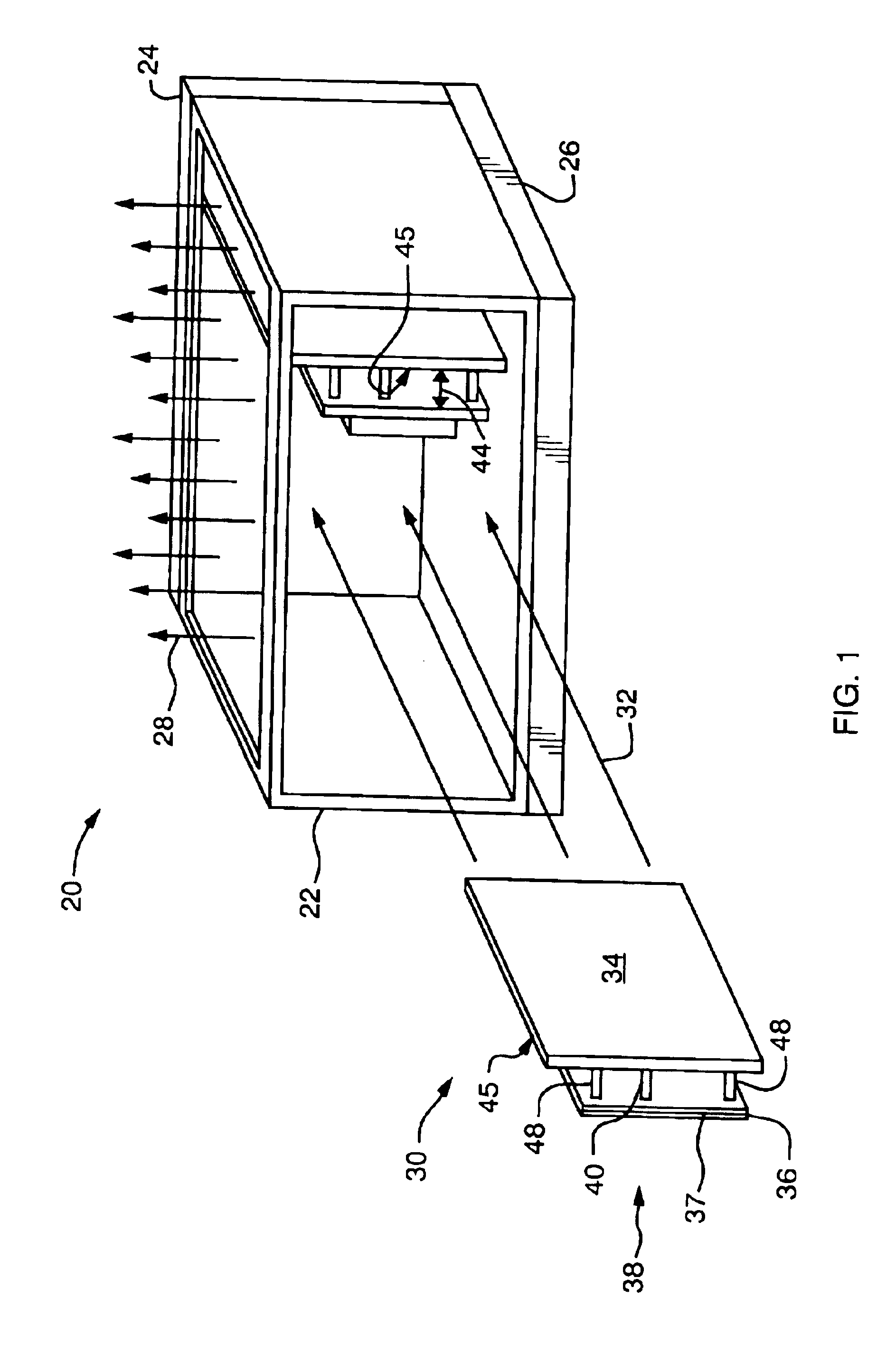
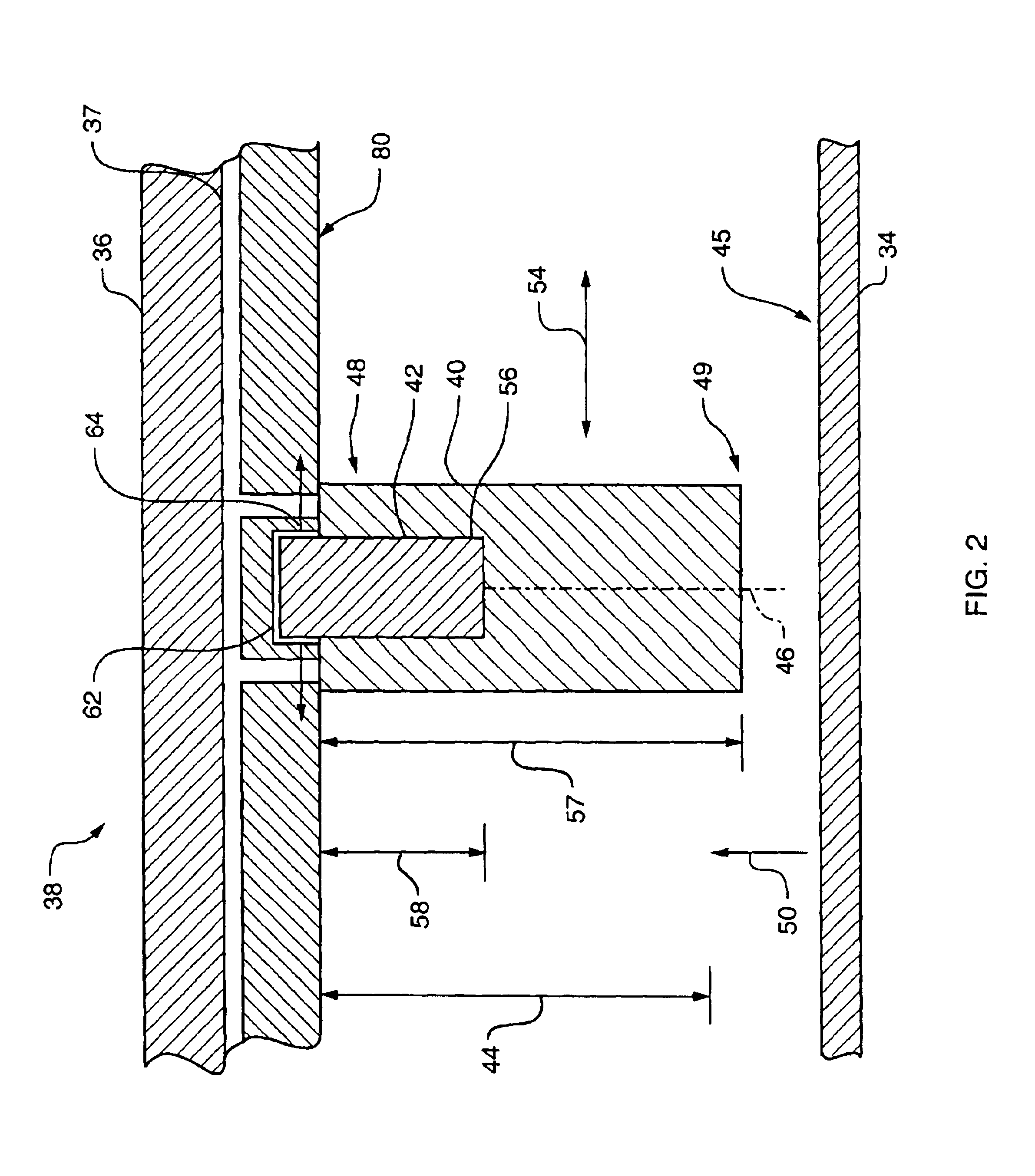
[0012]By contrast, embodiments of the present invention significantly overcome such deficiencies and provide mechanisms for grounding a circuit board. A grounding member support forms an interference or friction fit with an opening defined by the circuit board. A compliant,
electrically conductive grounding member couples to the grounding member support. The grounding member electrically couples a grounding layer of the circuit board with a support mount coupled to the circuit board. During
assembly,
insertion of the grounding member support within the opening defined by the circuit board creates an
expansive or lateral force on the opening. Furthermore, during assembly, the support mount compresses the compliant, electrically conductive grounding member against the circuit board. The
interference fit between the grounding member support and the opening along with compression of the grounding member between the circuit board and the support mount limits the amount of stress received by a surface of the circuit board. Such limitation of stress, in turn, limits potential damage to components mounted to the circuit board or to conductive layers within the circuit board. Because the grounding member support and grounding member limits the amount of stress directed against the circuit board, an assembler can configure the circuit board with as many grounding member supports and grounding members as necessary to reduce induction of current flow between grounding layer mesh locations of the circuit board without damaging the circuit board components or limiting the location of circuit board components on the circuit board.
[0013]In one arrangement, the grounding assembly has a circuit board having a conductive
ground plane defining an opening, a grounding member in electrical communication with the
ground plane, and a grounding member support forming an interference fit with the opening defined by the circuit board and configured to maintain electrical communication between the grounding member and the
ground plane of the circuit board. The grounding member is configured to compressibly engage a support mount substantially parallel to the circuit board to electrically couple the conductive ground plane of the circuit board to the support mount. Compression of the grounding member between the circuit board and the support mount limits the amount of stress generated by the grounding member against the circuit board, thereby limiting potential damage to components mounted to the circuit board or to conductive layers within the circuit board.
[0014]In one arrangement, an embodiment of the invention relates to a method for assembling a grounding assembly. In the method, an assembler forms a circuit board having a conductive ground plane and defining an opening. The assembler couples a grounding member support to the circuit board to form an interference fit with the opening defined by the circuit board and to maintain electrical communication between a grounding member and conductive ground plane of the circuit board. The assembler places the grounding member in mechanical communication with the grounding member support and in electrical communication with the conductive ground plane. The grounding member is configured to compressibly engage a support mount substantially parallel to the circuit board to electrically couple the conductive ground plane of the circuit board to the support mount. Compression of the grounding member between the circuit board and the support mount limits the amount of stress generated by the grounding member against the circuit board, thereby limiting potential damage to components mounted to the circuit board or to conductive layers within the circuit board.

