
Compact MR write structure

a write structure and compact technology, applied in the field of magnetic data storage systems, can solve the problems of increasing the flux rise time, hindering the write performance, and extra length, and achieve the effect of less space and less spa

Inactive Publication Date: 2005-05-17
WESTERN DIGITAL TECH INC
View PDF9 Cites 151 Cited by
  • Summary
  • Abstract
  • Description
  • Claims
  • Application Information

AI Technical Summary

Benefits of technology

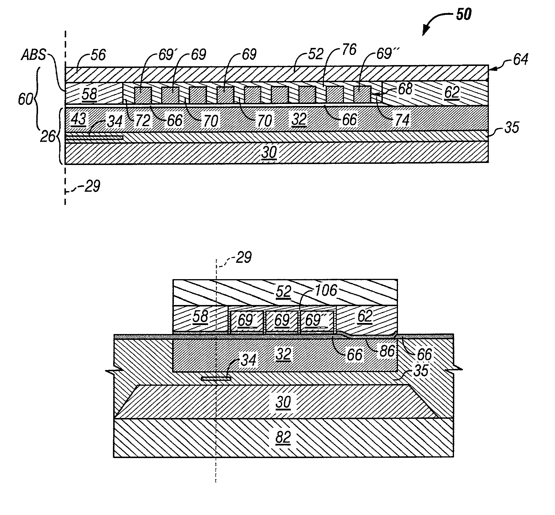
[0021]The present invention provides a compact structure for a write element of a read / write head of a magnetic data storage device. The structure includes both a substantially flat second pole, significantly less space between the coil and the backgap, and significantly less space between the coil and the pole pedestal. Additionally, a method for the fabrication of such a compact write element is provided.
[0024]This compact magnetic write structure is advantageous because it provides a substantially flat second pole without a slope region. Eliminating the slope region serves to both reduce the magnetostrictive induced resistance to magnetization changes in the yoke, and to reduce the stack height. Both of these changes reduce the flux rise time and improve writing performance. The structure is further advantageous for limiting the separation between the pole pedestal and the coil to no greater than about 2.0 microns, thereby reducing the yoke length for further writing performance enhancement. The embodiment in which the separation between the backgap and the coil to no greater than about 2.0 microns is similarly advantageous for further reducing the yoke length. Still another advantage is the ability to fabricate the structure without retaining photoresist as an insulator. This is also advantageous for lowering the flux rise time by reducing unwanted stresses in high Bs magnetic materials caused by large mismatches in coefficients of thermal expansion.
[0025]Yet another embodiment of the present invention is directed to a method for manufacturing a magnetic write structure. The method includes providing a substrate including a conductive shield layer and an insulating write gap layer. The conductive shield layer defines a plane, and the insulating write gap layer at least partially covers the conductive shield layer. The method further includes forming over the substrate a self-aligned array comprising a plurality of components including a conductive pole pedestal and a coil. The pole pedestal and the coil contact the write gap layer, and the separation between the pole pedestal and the coil is no greater than about 2.0 microns. Additionally, the method includes forming a conductive pole layer over the self-aligned array. The pole layer is in contact with the pole pedestal and defines a plane that is substantially parallel to the plane of the conductive shield layer. The present invention further includes a planarization step prior to the formation of the pole layer helping to ensure that the plane of the pole layer is substantially parallel to the plane of the conductive shield layer.
[0027]These methods for manufacturing magnetic write structures are advantageous because they incorporate a self-aligned array. A self-aligned array allows the pole pedestal and the coil to be formed with the same mask, thereby allowing these two components to be formed as close together as masking technology will allow without having to leave excess space between them to allow for the possible misalignment of successive masks. Embodiments incorporating a backgap also take advantage of the self-aligned array to minimize the space between the backgap and the coil. A further advantage of the self-aligned array is that it reduces the total number of masking operations needed to form a magnetic write structure, thus saving time and reducing manufacturing costs.
[0028]Another advantage of this manufacturing method derives from the planarization step preceding the formation of the pole layer. The planarization achieves three important goals. The first goal is to expose the backgap and the second pole pedestal. The second is to reduce the overall stack height of the finished write structure, improving the write performance of the finished device. The third goal served by the planarization step is that the pole layer formed over the planarized surface is itself substantially flat and substantially parallel to the plane of the conductive shield layer. This serves to simplify the geometry of the pole layer, thereby reducing or substantially eliminating domain striping and further improving write performance of the finished device.

Problems solved by technology

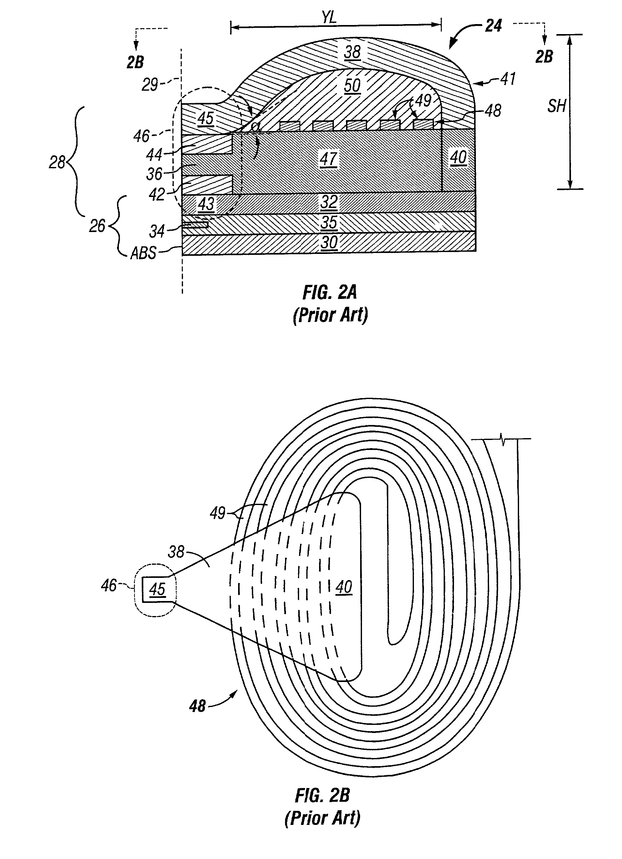
These separations add extra length to the yoke length YL that increases the flux rise time and hinders write performance.
Increasing the stack height SH makes it difficult to control the track width within narrow set tolerances, decreasing the production yield.
Consequently, increasing the apex angle α has the effect of increasing the stack height SH to the detriment of write performance.
The second pole 38 is typically formed by sputtering or plating, techniques well suited for producing flat layers, but not as well suited for forming complex surfaces.
Consequently, a further problem associated with the apex angle α is lower production yields resulting from the difficulties encountered in producing uniformity in the second pole 38, especially in the slope region.
The trend towards higher density recording in the disk drive industry has forced a number of materials changes in the components of the drives, which has, in turn, created additional problems.
In particular, in order to achieve higher data densities on the surface of the magnetic disk 16, the traditional magnetic media have not been found to be sufficient.
However, Permalloy has an unacceptably low Bs for use in high density recording.
These higher magnetostriction values create additional problems for high density recording applications.
The retention of photoresist as an insulator in some prior art devices is especially troublesome in this regard, as photoresist has a relatively large coefficient of thermal expansion.

Method used


Image

  • Compact MR write structure
  • Compact MR write structure
  • Compact MR write structure

Examples


Embodiment Construction

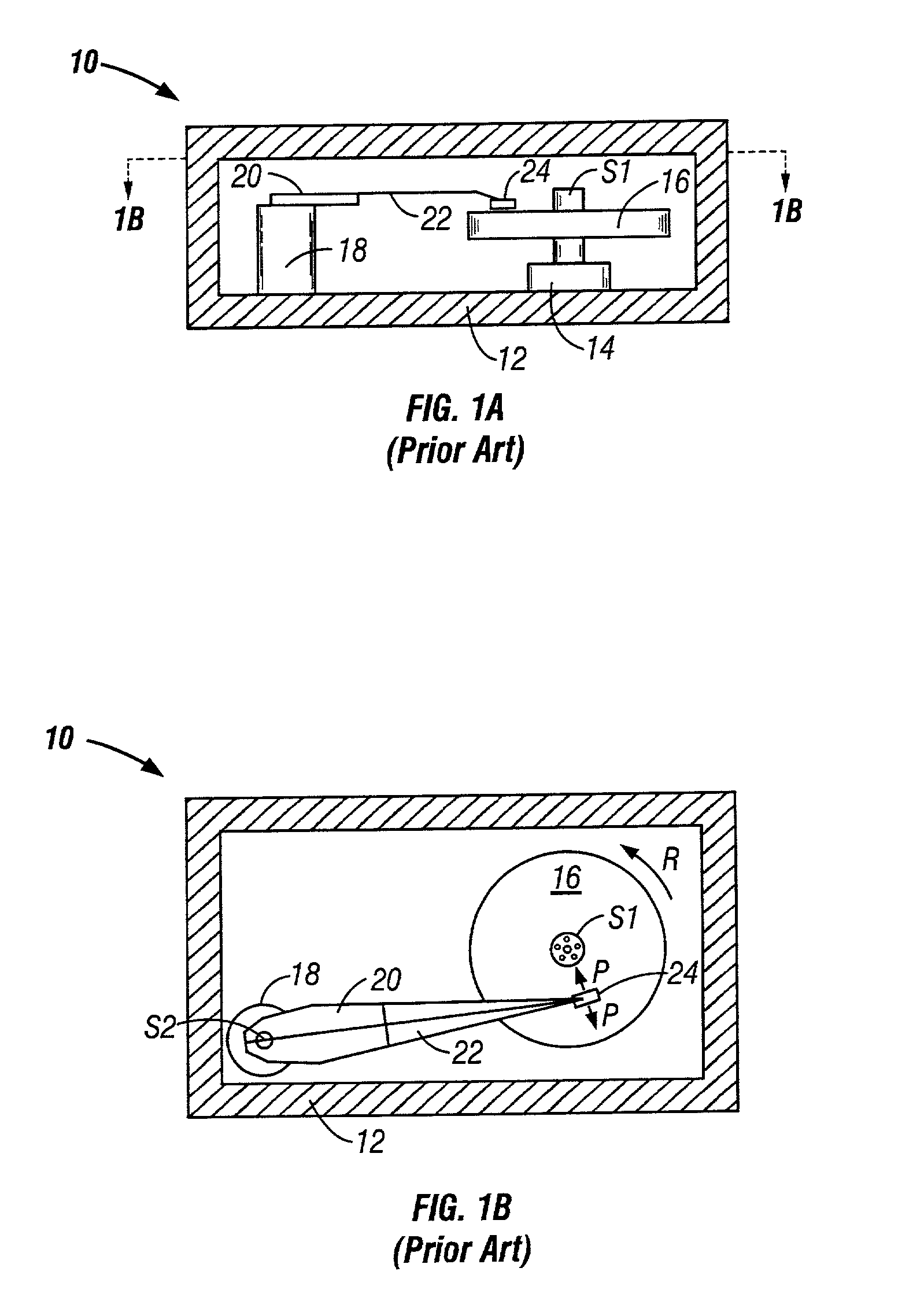
[0045]FIGS. 1A, 1B, 2A, 2B, 3A–3C, and 4 were discussed with reference to the prior art.

[0046]FIG. 5 is a cross-sectional view of a read / write head 50 according to an embodiment of the present invention, including a read element 26 and a write element 60. Edges of the read element 26 and write element 28 also define an air bearing surface ABS, in a plane 29, which can be aligned to face the surface of the magnetic disk 16. The read element 26 includes a first shield 30, a conductive shield layer 32, which functions as a second shield, and a read sensor 34 that is located within a dielectric medium 35 between the first shield 30 and the conductive shield layer 32. Embodiments of the present invention may include a read sensor 34 that may be any type magnetoresistive sensor to detect magnetic field signals from a magnetic disk 16.

[0047]The write element 60 includes conductive shield layer 32, which functions as a first pole, and a second pole 52. The conductive shield layer 32 include...


PUM


Abstract

A compact write element includes a conductive shield layer, an insulating write gap layer, a pole pedestal, a coil, and a conductive pole layer, and, in some embodiments also includes a backgap. The pole pedestal and the coil, and, in some embodiments the backgap, constitute a self-aligned array of components that may be formed in a single masking operation to allow for very tight tolerances between the components for a shorter yoke length. The pole layer is substantially flat and parallel to the conductive shield layer, providing for a shorter stack height. Also, a compact MR read / write head includes such a write element and a magnetic data storage and retrieval system includes the compact MR read / write head having such a write element.

Description

CROSS REFERENCE TO RELATED APPLICATION[0001]This application is a Divisional of U.S. application Ser. No. 09 / 336,646, filed 18 Jun. 1999 now U.S. Pat. No. 6,466,402, which is hereby incorporated by reference in its entirety.BACKGROUND OF THE INVENTION[0002]This invention relates generally to magnetic data storage systems, more particularly to magnetoresistive read / write heads, and most particularly to an especially compact write structure.[0003]Magnetic disk drives are used to store and retrieve data for digital electronic apparatuses such as computers. In FIGS. 1A and 1B, a magnetic disk data storage system 10 includes a sealed enclosure 12, a disk drive motor 14, and a magnetic disk, or media, 16 supported for rotation by a drive spindle S1 of motor 14. Also included are an actuator 18 and an arm 20 attached to an actuator spindle S2 of actuator 18. A suspension 22 is coupled at one end to the arm 20, and at its other end to a read / write head or transducer 24. The transducer 24 ty...

Claims


Application Information

Patent Timeline
IPC IPC(8): G11B5/39G11B5/31
CPCG11B5/3113G11B5/3967G11B5/313
Inventor CRUE, JR., BILL W.SHI, ZHUPEITONG, LIJUNCORONA, CARLOS
Owner WESTERN DIGITAL TECH INC
Learn More