Process for making angled features for nanolithography and nanoimprinting

a nanolithography and nanoimprinting technology, applied in the field of semiconductor device manufacturing, can solve the problems of unsatisfactory perpendicular structure, frustrated production to date, and inability to achieve consistent precise angles, and achieve the effect of facilitating the insertion and extraction of the nanoimprinting templa

Inactive Publication Date: 2005-05-24
HEWLETT PACKARD DEV CO LP
View PDF5 Cites 24 Cited by
  • Summary
  • Abstract
  • Description
  • Claims
  • Application Information

AI Technical Summary

Benefits of technology

[0014]In yet another embodiment, the invention may provide a directional ion etching process for making angled features in a nanoimprinting template for use with a soft polymer including: depositing at least one layer of undefined template material upon a wafer substrate; depositing a photoresist upon the undefined template material layer; masking the photoresist to provide a plurality of substantially identical photoresist protected areas, the photoresist being developed to remove the photoresist from the non-protected areas, thereby exposing and defining portions of the template layer; anisotropic reactive ion etching at a high angle relative to the wafer substrate to substantially remove the exposed portions of the template layer; and removing the photoresist from the protected area thereby providing a nanoimprinting template including a plurality of substantially identical angled features of template material, wherein the angle of the features facilitates insertion and extraction of the nanoimprinting template.

Problems solved by technology

While the widespread application of semiconductors exemplifies the functionality of perpendicular structures, there are known situations where the perpendicular structure is not ideal.
While it has been understood that tilting the pillars would expose at least one side, and thereby increase the apparent polarization effect upon the crystal, difficulties in reducing pillar size and in achieving consistent precise angles have frustrated their production to date.
The masking process and the developing process do have inherent error margins.
Further, as the creation of a mask is typically complex and cost intensive, use of a single large mask to mask an entire substrate all at once may not be desired.
As a result a smaller mask may be used repeatedly to achieve the affect of a single large mask, however, misalignment of the repeated maskings may waste material and / or result in an unusable wafer.
As the structures provided on the template extend perpendicularly and are of a small scale, it is often difficult to affectively apply the template.
Rotation of the template during application or removal is likely to damage the template and / or improperly skew the negative impression.
Any particulates incorporated into the resist or left behind on the template / stamp lead to eventual wearing out of the stamp and also defects in the printed resist.
While rolling the template into and out of the soft polymer would greatly reduce the stress imposed upon the surfaces, the ability to provide sufficiently strong, small and angled features upon a template has proven unreliable.

Method used


Image

  • Process for making angled features for nanolithography and nanoimprinting
  • Process for making angled features for nanolithography and nanoimprinting
  • Process for making angled features for nanolithography and nanoimprinting

Examples


Embodiment Construction

[0020]Before proceeding with the detailed description, it is to be appreciated that the present invention is not limited to use or application with a specific type of magnetic memory. Thus, although the present invention is, for the convenience of explanation, depicted and described with respect to typical exemplary embodiments, it will be appreciated that this invention may be applied with other types of magnetic memory.

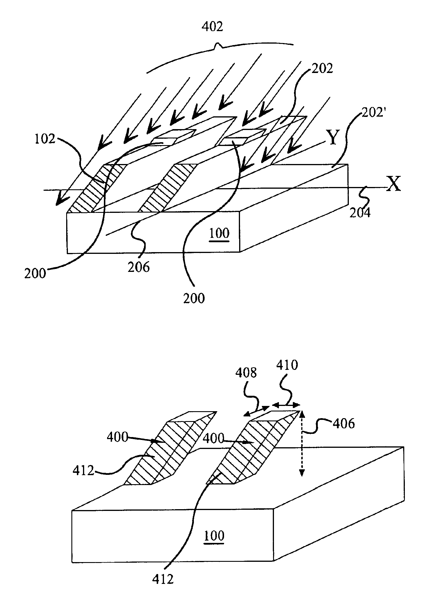
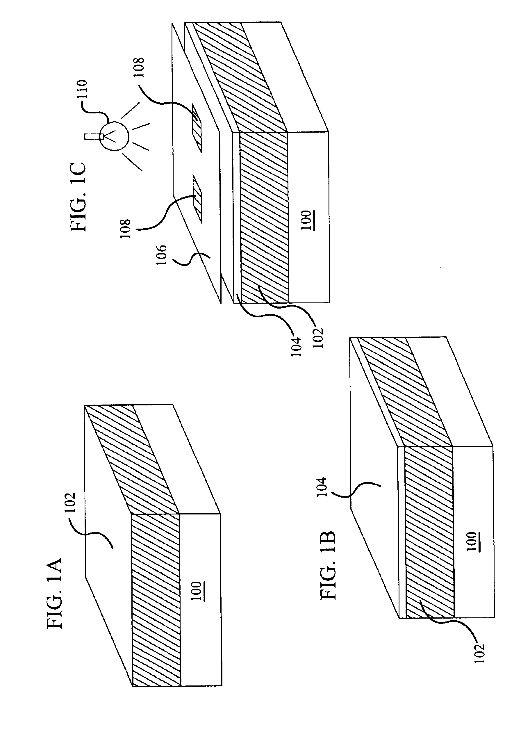
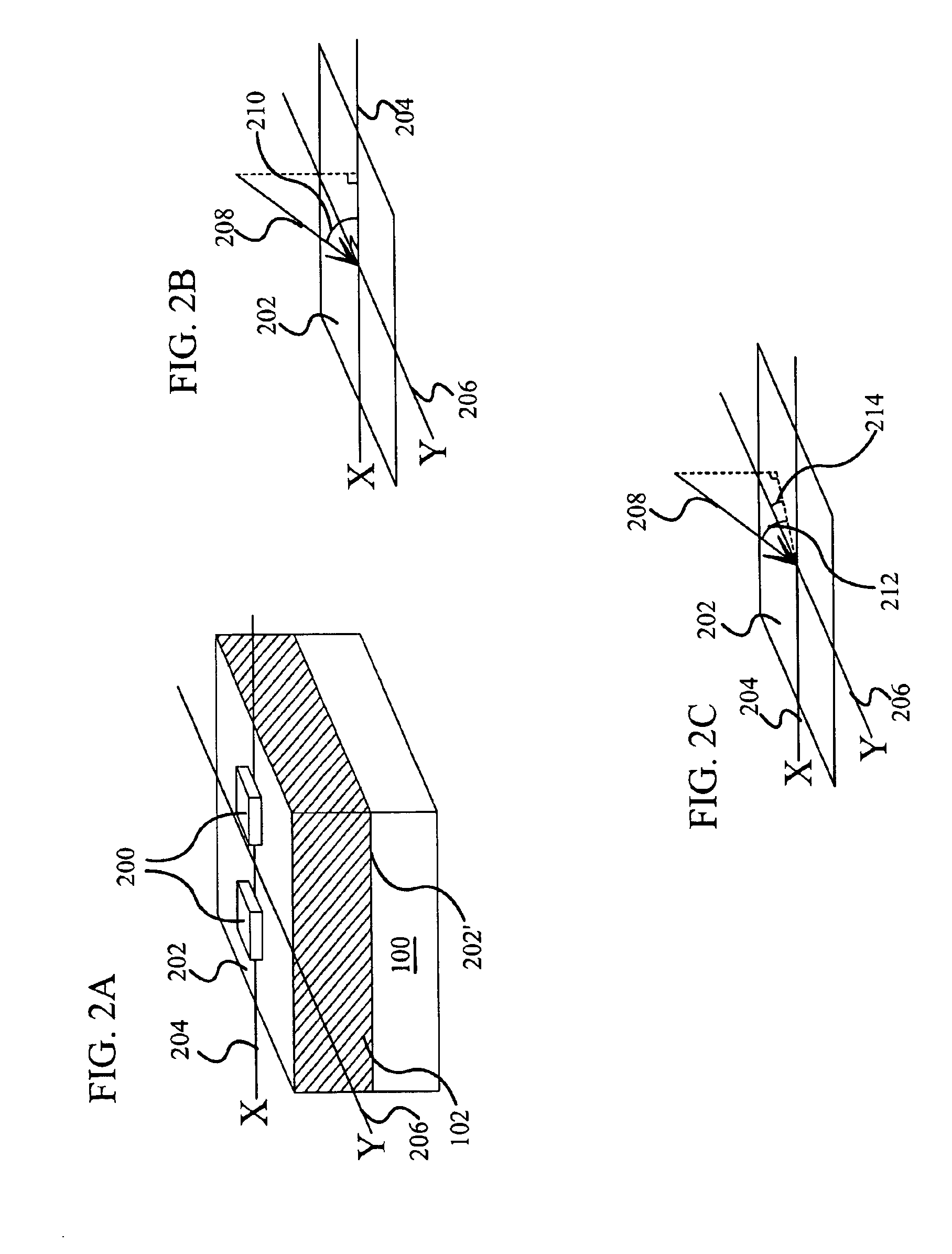
[0021]Referring now to the drawings, FIGS. 1 through 4 conceptually illustrate an ion etching (also known as plasma etching) process for making angled features according to an embodiment of the present invention. It will be appreciated that the described process need not be performed in the order in which process for providing it is herein described, but that this description is merely exemplary of one preferred method of fabricating nano-scale angled features.

[0022]In at least one embodiment, the fabrication process may be commenced upon a semiconductor substrate w...


PUM

PropertyMeasurementUnit
aspect ratioaaaaaaaaaa
angleaaaaaaaaaa

Abstract

This invention provides a directional ion etching process for making nano-scaled angled features such as may be used, for example, in liquid crystal displays and or nanoimprinting templates. In a particular embodiment a semiconductor wafer substrate is prepared with at least one layer of material. A photoresist is applied, masked, exposed and developed. Anisotropic ion etching at a high angle relative to the wafer is performed to remove portions of the non protected material layer. The remaining photoresist caps shadow at least a portion of the material layer, and as the ion etching is performed at an angle, the protected portions of the material layer also appear at an angle.

Description

FIELD OF THE INVENTION[0001]This invention relates generally to the manufacture of semiconductor devices and in particular to an improved method of making angled pillars for nanolithography and / or nano imprinting.BACKGROUND OF THE INVENTION[0002]Traditional semiconductor fabrication techniques construct structures that are generally comprised of orthogonal elements. Transistors, conductors, isolators, or other structures may be visualized as a child's set of wooden building blocks. They may be placed one atop another and in appropriate cases may overlap, but when viewed from above, traditionally the top surfaces are visible while the perpendicular side surfaces are not.[0003]While the widespread application of semiconductors exemplifies the functionality of perpendicular structures, there are known situations where the perpendicular structure is not ideal. At least two examples can be readily found with respect to liquid crystal displays and the mass production of precise nanometer ...

Claims


Application Information

Patent Timeline
Patent Type & Authority Patents(United States)
IPC IPC(8): H01L21/02H01L21/302G02F1/1337
CPCG02F1/13378B81C99/009B81C1/00626B81B2203/0361
Inventor SHARMA, MANISH
Owner HEWLETT PACKARD DEV CO LP
Why Eureka
Try Eureka