
Isolated FET drive utilizing Zener diode based systems, methods and apparatus

a technology of zener diodes and drives, applied in the direction of diodes, oscillator generators, pulse techniques, etc., can solve the problems of complex base control circuitry, inability to easily transport transistors, and inability to achieve the effect of facilitating the inherent quality of pre-existing circuits, simplifying circuitry and parts, and facilitating gated semiconductor devices

Inactive Publication Date: 2005-05-24
NORTHROP GRUMMAN SYST CORP
View PDF12 Cites 16 Cited by
  • Summary
  • Abstract
  • Description
  • Claims
  • Application Information

AI Technical Summary

Benefits of technology

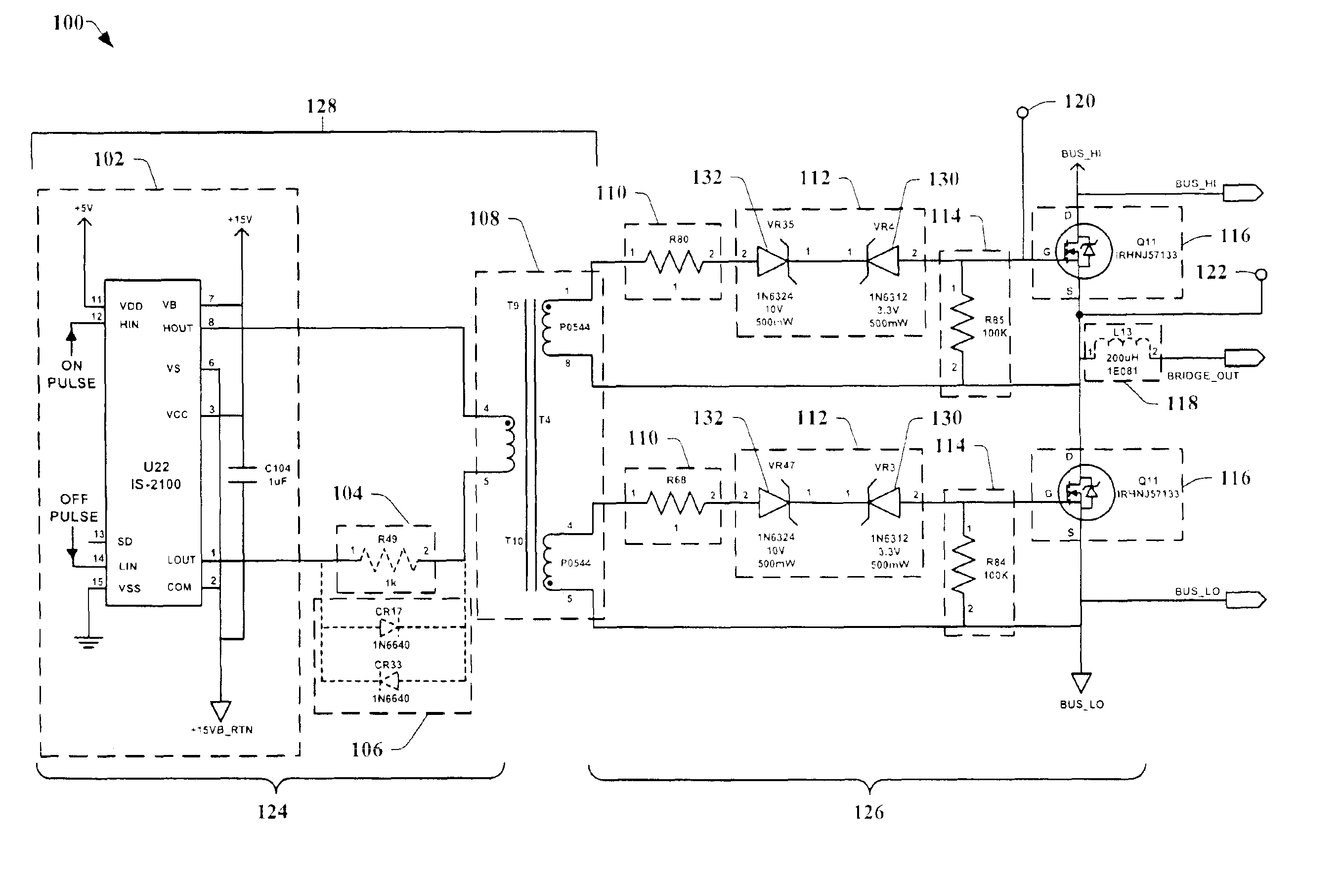
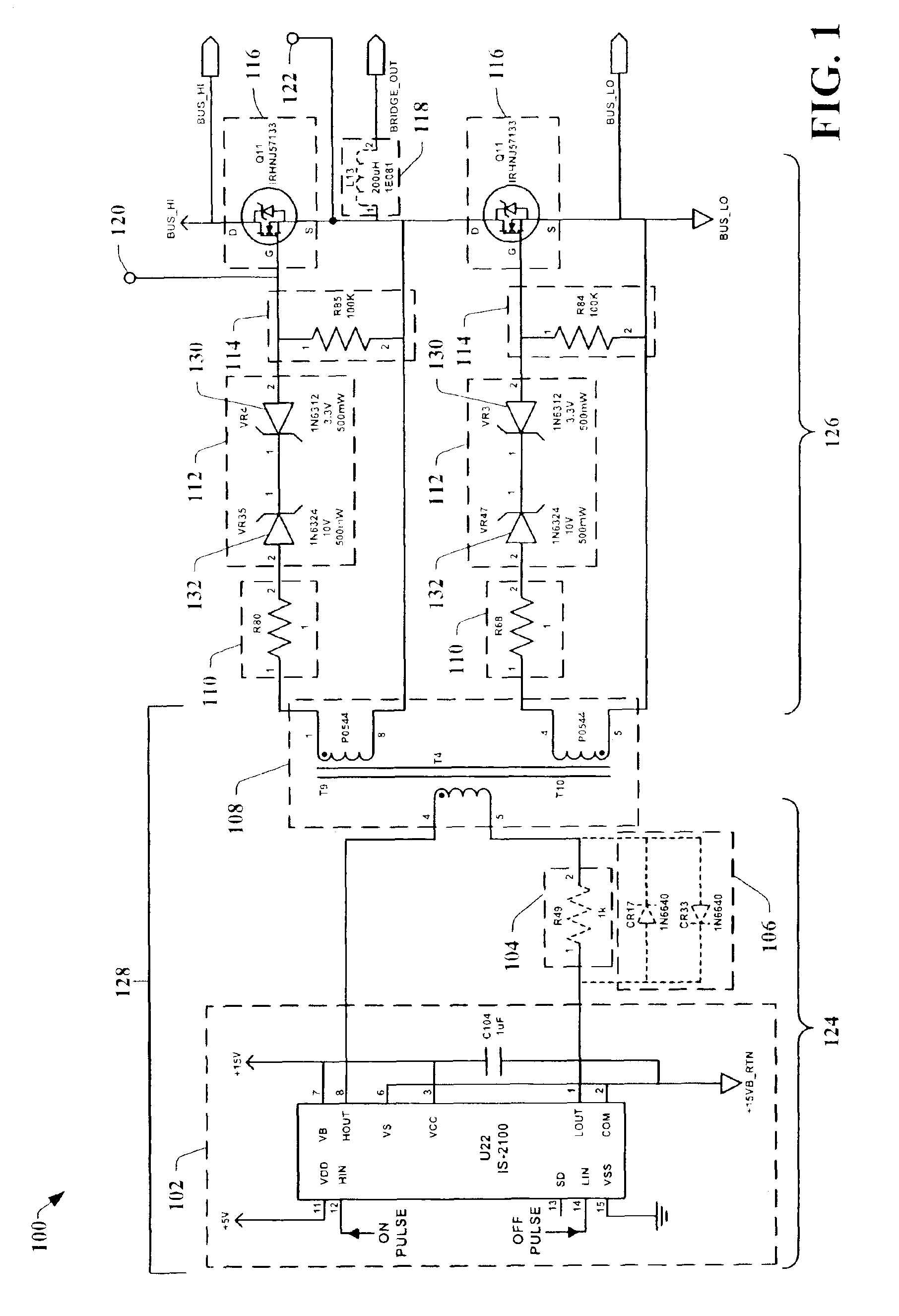
[0014]The present invention relates generally to semiconductor device control, and, in particular, to controlling a gated semiconductor device utilizing an isolated gate driver. By employing the present invention, the semiconductor device is driven with a more advantageous and less complicated gate driver. The present invention facilitates controlling gated semiconductor devices by simplifying both the circuitry and parts required. The subject invention also facilitates the inherent quality of pre-existing circuits by providing better control with less complex, higher dependability parts.
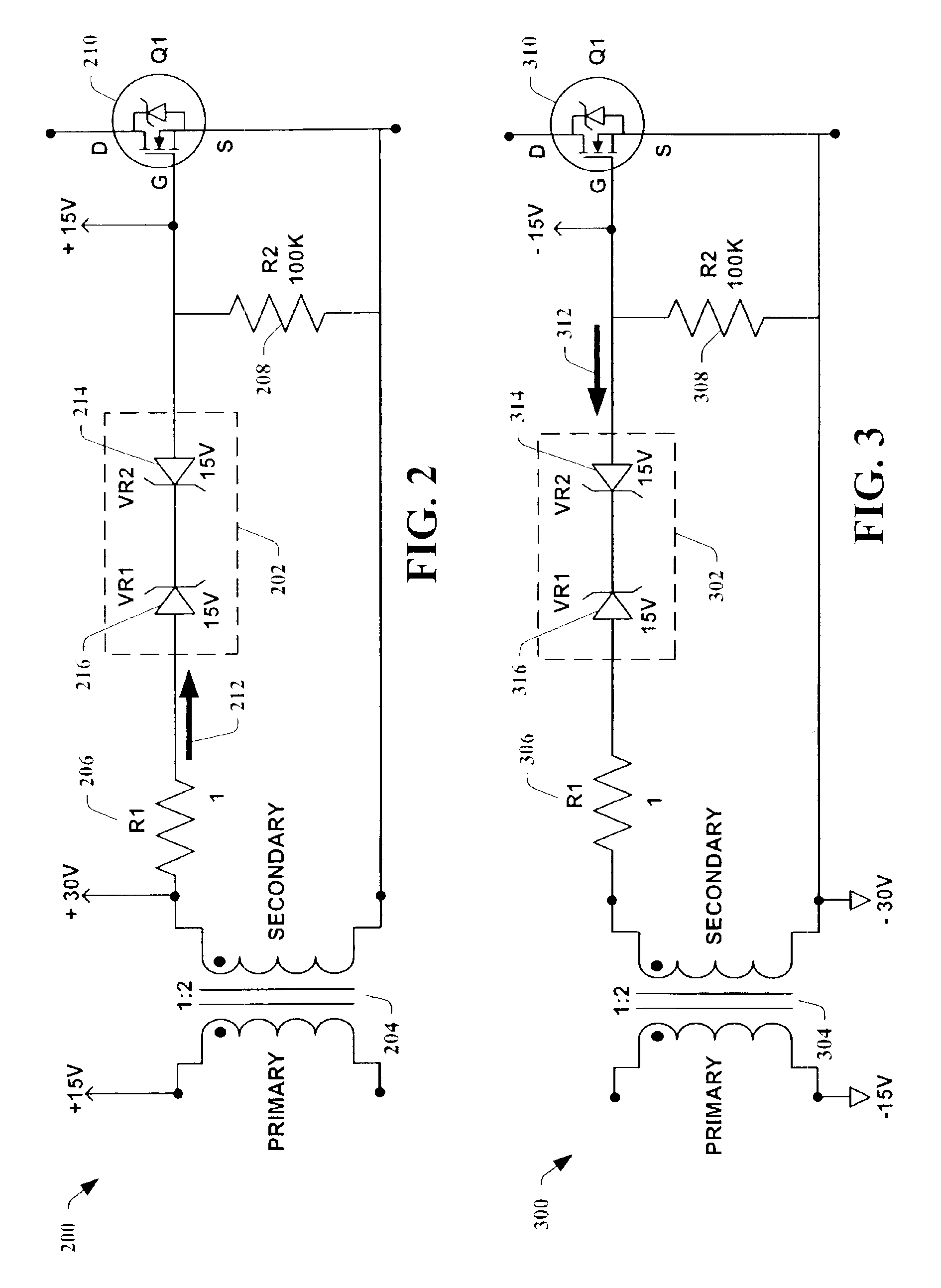
[0015]More particularly, the subject invention utilizes opposing current inhibiting elements capable of controlling current flow until a predetermined voltage level is obtained across the current inhibiting element opposing the current flow. A difference of an isolated input voltage level and the predetermined voltage level approximates a gate voltage potential employed to drive a gate input of a semiconductor device. This is accomplished, in one instance of the present invention, by employing Zener diodes in an opposing fashion to produce the gate voltage potential. Zener diode breakdown voltages provide the predetermined voltage levels necessary to properly control the gated semiconductor device during gate charge and discharge cycles. Thus, in accordance with the subject invention, a gate of a semiconductor device, such as a MOSFET and / or IGBT and the like, can be driven by a less complex, higher reliability isolated driver. Since enhanced characteristics are obtained utilizing this type of semiconductor device, the present invention reduces implementation costs, increases quality, and simplifies part complexity.

Problems solved by technology

Prior to this time, circuits requiring amplification of signals were forced to utilize bulky vacuum tubes for this task.
This led to new portable devices, such as the transistor radio, that before the transistor could not have been transported easily.
The BJT excels in “on” characteristics, but its base control circuitry needs to be complex for proper operation, and it is not as good in fast switching as the MOSFET.
The silicon dioxide layer between the gate and the source regions can be easily penetrated, resulting in device failure, if the voltage between the gate and source exceeds 20 volts, even with low current.

Method used


Image

  • Isolated FET drive utilizing Zener diode based systems, methods and apparatus
  • Isolated FET drive utilizing Zener diode based systems, methods and apparatus
  • Isolated FET drive utilizing Zener diode based systems, methods and apparatus

Examples


Embodiment Construction

[0028]The present invention is now described with reference to the drawings, wherein like reference numerals are used to refer to like elements throughout. In the following description, for purposes of explanation, numerous specific details are set forth in order to provide a thorough understanding of the present invention. It may be evident, however, that the present invention may be practiced without these specific details. In other instances, well-known structures and devices are shown in block diagram form in order to facilitate describing the present invention.

[0029]As used in this application, the term “computer component” is intended to refer to a computer-related entity, either hardware, a combination of hardware and software, software, or software in execution. For example, a computer component may be, but is not limited to being, a process running on a processor, a processor, an object, an executable, a thread of execution, a program, and / or a computer. By way of illustrat...


PUM


Abstract

The present invention provides a system, apparatus and methodology for semiconductor device gate control utilizing a gate driver circuit 112 having opposing current inhibiting elements 130, 132 capable of controlling current flow until a predetermined voltage level is obtained across the current inhibiting element opposing the current flow. A difference of an isolated input voltage level and the predetermined voltage level approximates a gate voltage potential employed to drive a gate input of a semiconductor device. This is accomplished, in one instance of the present invention, by employing Zener diodes in an opposing fashion to produce the gate voltage potential. Zener diode breakdown voltages provide the predetermined voltage levels necessary to properly control the gated semiconductor device during gate charge and discharge cycles.

Description

BACKGROUND OF THE INVENTION[0001]1. Field of the Invention[0002]The present invention relates to a system, apparatus and methodology for semiconductor device control, and in particular to controlling semiconductor devices utilizing an isolated FET drive based on Zener diodes.[0003]2. Discussion of the Related Art[0004]Semiconductors have permeated into every aspect of modern society. They are the building blocks used to create everything from the information super-highway to the electronic timer in the family toaster. Generally, any device that is considered “electronic” utilizes semiconductors. These often-unseen components help to reduce the daily workload, increase the safety of our air traffic control systems, and even let us know when it is time to add softener to the washing machine. Modern society has come to rely on these devices in almost every product produced today. And, as we progress further into a technologically dependent society, the demand for increased device speed...

Claims


Application Information

Patent Timeline
Patent Type & Authority Patents(United States)
IPC IPC(8): H03K17/689H03K17/691H03K17/30
CPCH03K17/691H03K17/302
Inventor BECK, MARTIN E.
Owner NORTHROP GRUMMAN SYST CORP
Learn More