Low offset and low glitch energy charge pump for PLL-based timing recovery systems

a technology of energy charge pump and timing recovery system, which is applied in the direction of electrical apparatus, pulse automatic control, etc., can solve the problems of difficult type phase-lock-loop circuit, difficult to maintain perfect phase-lock vco to data, and general impracticality of transmitting the requisite sampling clock signal separate from the transmitted datastream, etc., to achieve the effect of maintaining the stability of vco lock

Inactive Publication Date: 2005-05-24
QUALCOMM INC
View PDF4 Cites 25 Cited by
  • Summary
  • Abstract
  • Description
  • Claims
  • Application Information

AI Technical Summary

Benefits of technology

[0015]A high-speed phase lock loop circuit includes a high precision charge pump which functions to maintain the stability of VCO lock by providing source and sink pump currents which are substantially zero over phase correction cycle. The uniformity of source and sink currents is imposed by valuating the voltages at the common drain nodes of the charge pump's first and second parallel conduction paths by a feedback element. The feedback element controls the value of an “adjust” current source so as to drive the two common drain nodes to an equi-potential level.
[0017]Each of the two parallel current paths is constructed of an upper switch connected in series with a lower switch with the common nodes of each parallel current path defining a respective output node. The upper switch may be constructed of an N-channel transistor, while the lower switch may be constructed of a P-channel transistor. The charge pump includes a feedback element coupled between the output nodes and an “adjust” current source which functions to balance currents in the two parallel current paths so as to minimize DC offsets at the circuit output.
[0020]An amplifier, such as a transconductance amplifier, has first and second inputs coupled, respectively, to the first and second output nodes and an output connected to control operation of an “adjust” current source. The “adjust” current source might be provided separately or, might be incorporated into the charge pump's “pump-up” or “pump-down” current sources directly. The amplifier thus forces the common drain nodes of each of the current paths to be maintained at an equi-potential value with respect to one another. By maintaining the dump capacitor node and the zero capacitor node at the same voltage during operation of the charge pump, independent of the output voltage of the charge pump, non-linearities and DC offsets developed by the charge pump are minimized.

Problems solved by technology

Given the bandwidth constraints imposed on most modern data communication systems, it is generally impractical to transmit the requisite sampling clock signal separate from the transmitted datastream.
Maintaining perfect phase-lock VCO to data, however, is particularly difficult for conventional prior art-type phase-lock-loop circuits operating in the GHz range, because of the internal construction of conventional prior art-type charge pump circuits.
In addition, the source and sink current waveforms, of such conventional charge pump circuits, exhibit significant amounts of offset and “glitch errors” which cause the source and sink current waveforms to be non-symmetrical.
This non-symmetry necessarily results in a residual charge being left on the filter capacitor at the end of a correction cycle and further causes a non-zero increment to the control voltage Vc to the VCO.
This DC offset current tends to perturb the system in one direction or the other and results in timing jitter at the output of the VCO.
Accordingly, prior art-type charge pump circuits do not provide a smooth, constant and symmetrical response characteristic between their source and sink currents during phase lock, thus introducing variation to the loop filter and, consequently the VCO output.

Method used


Image

  • Low offset and low glitch energy charge pump for PLL-based timing recovery systems
  • Low offset and low glitch energy charge pump for PLL-based timing recovery systems
  • Low offset and low glitch energy charge pump for PLL-based timing recovery systems

Examples


Embodiment Construction

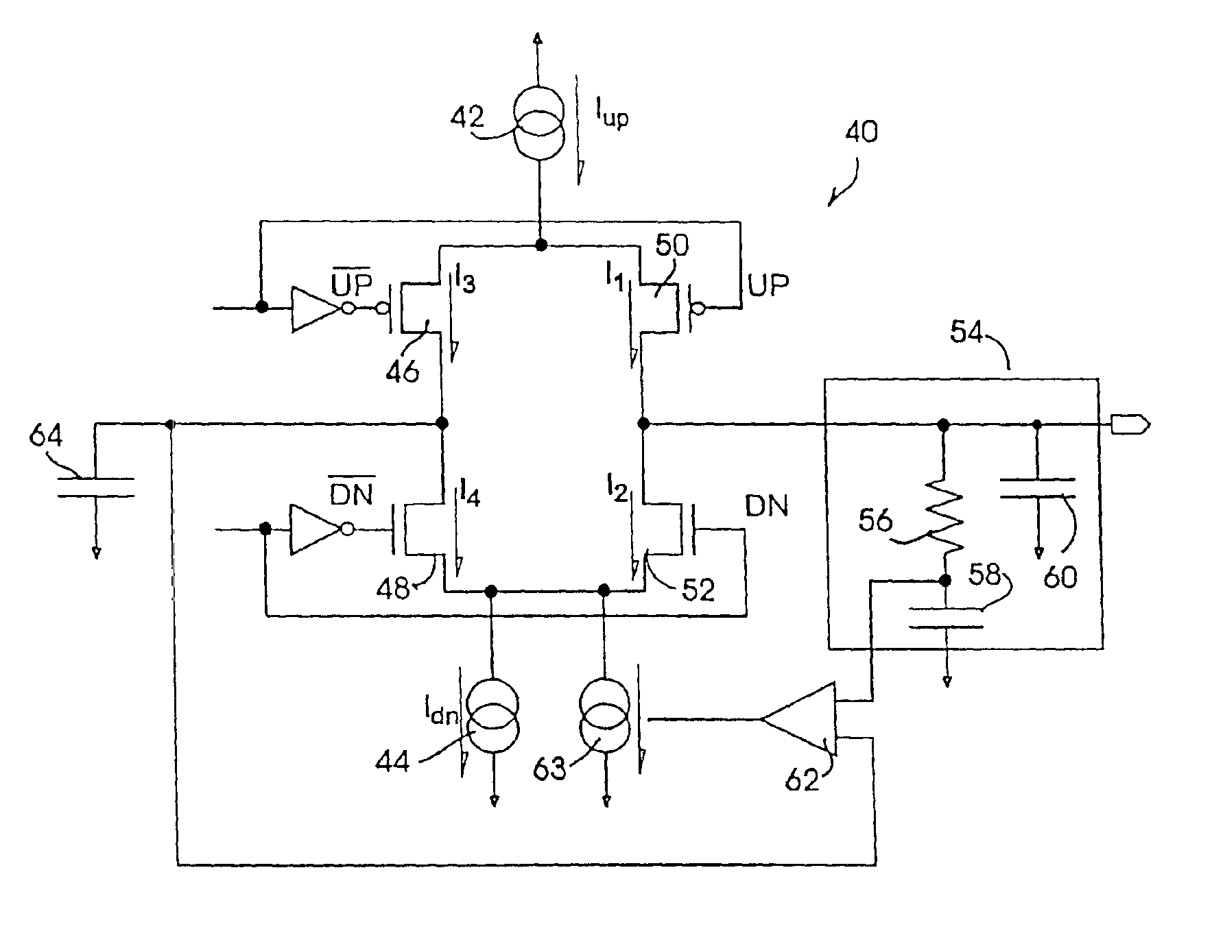
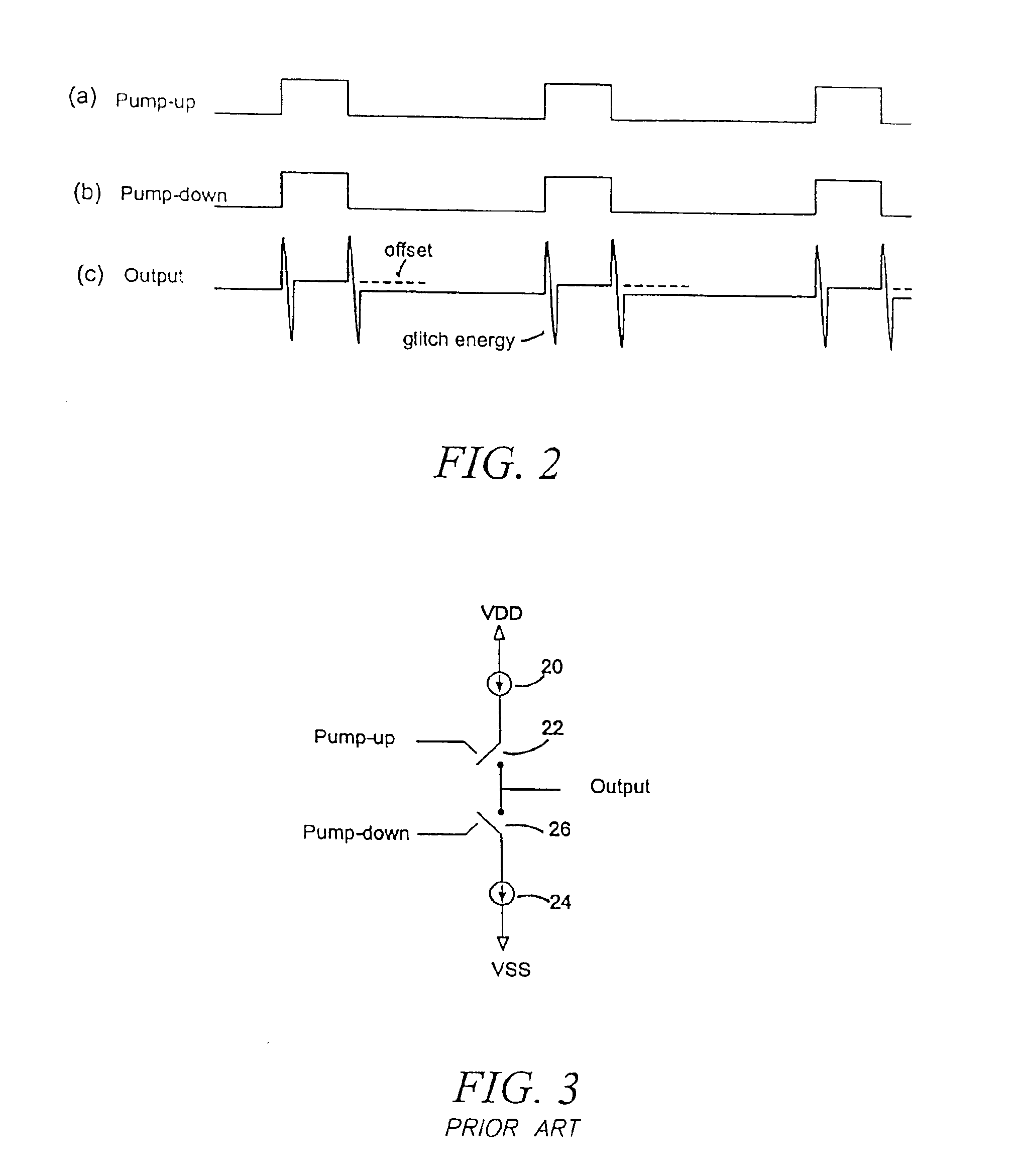
[0027]In practical terms, lack of perfect symmetry between sourced and sunk charge pump current selectively adds a small component (a DC offset component, a glitch error component, or both) to the control voltage Vc provided to a VCO. These error components selectively shift frequency of a VCO relative to its nominal center frequency. Any offset from the center frequency will cause a phase detector's data capture window to shift, thus allowing a portion of data pulse position distribution to fall outside the detection window, and consequently increasing the system's bit error rate.

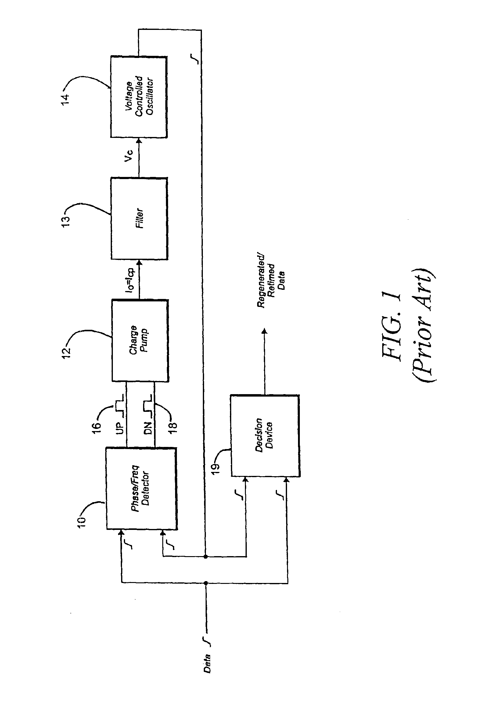
[0028]FIG. 4 illustrates, in simplified semi-schematic circuit diagram form, a typical prior art-type three-state charge pump, coupled to receive PUMP UP and PUMP DN signals from a phase detector 28. The charge pump is implemented as two switched current sources 30 and 32 driving a capacitor 34 which, in turn, defines an output voltage (VOUT or Vc). The charge pump switches are disposed as an upper and low...


PUM


Abstract

A high precision charge pump used in a phase-lock-loop incorporating a phase / frequency detector is designed and constructed to substantially eliminate the effects of DC offset and glitch errors on the charge pump output current. The high precision charge pump is constructed of parallel current paths each having a central node which is, in turn, connected to a feedback element. The feedback element defines a feedback current which is applied to the charge pump so as to maintain the two central nodes at an equi-potential level and to maintain the value of the pump-down current exactly equal to the value of the pump-up current output by the device.

Description

CROSS-REFERENCE TO RELATED APPLICATIONS[0001]This application is a continuation of application Ser. No. 09 / 649,197, filed Aug. 28, 2000, now U.S. Pat. No. 6,326,852, entitled LOW OFFSET AND LOW GLITCH ENERGY CHARGE PUMP FOR PLL-BASED TIMING RECOVERY SYSTEMS, which is a continuation of 09 / 398,101, filed Sep. 16, 1999, now U.S. Pat. No. 6,181,210, entitled LOW OFFSET AND LOW GLITCH ENERGY CHARGE PUMP FOR PLL-BASED TIMING RECOVERY SYSTEMS, and which is related to provisional application Ser. No. 60 / 101,555, filed Sep. 21, 1998, entitled LOW OFFSET AND LOW GLITCH ENERGY CHARGE PUMP DESIGN, all commonly owned by the Assignee of the present invention.FIELD OF THE INVENTION[0002]The present invention is directed to high speed data transmission and conversion systems and, more particularly, to a system for and a method of controlling the average current output of a charge pump such that glitch energy and offset voltage errors are minimized.BACKGROUND OF THE INVENTION[0003]The past several y...

Claims


Application Information

Patent Timeline
Patent Type & Authority Patents(United States)
IPC IPC(8): H03L7/089H03L7/08
CPCH03L7/0898H03L7/0896
Inventor WAKAYAMA, MYLES H.
Owner QUALCOMM INC
Why Eureka
Try Eureka