PCB structure for scope unit of electronic endoscope

a technology of electronic endoscope and pcb, which is applied in the field of pcb structure for electronic endoscope, can solve the problems of troublesome large scope unit, troublesome electrical connection of circuit pattern portions to other parts of the scope with wires, and large scope burden on the operator, so as to improve the pcb structure and facilitate the electrical connection between two patterns provided on piled pcbs.

Inactive Publication Date: 2005-05-24
ASAHI KOGAKU KOGYO KK
View PDF4 Cites 92 Cited by
  • Summary
  • Abstract
  • Description
  • Claims
  • Application Information

AI Technical Summary

Benefits of technology

[0007]The present invention is advantageous in that an improved PCB structure is provided, in which the electrical connection between two patterns respectively provided on piled PCBs can be done relatively easily, and wires connecting the patterns may not be broken easily.

Problems solved by technology

The large scope unit is troublesome in handling, i.e., in each of operating, carrying and storage, the larger scope is burdensome to the operator.
However, in such a structure, since one circuit pattern is divided into two patterns, if the two PCBs are arranged such that large size electrical elements of the two PCBs are arranged to face outside and the circuit patterns of the two PCBs face each other, it is very troublesome to electrically connect portions of one circuit pattern to portions of the other with wires.
Specifically, after the two PCBs are piled, it is difficult to wire.
For example, soldering the wires are difficult with the PCBs piled if the printed patterns face each other.
However, in such a case, the wires are longer than the clearance between the two PCBs, depending on the configuration of the PCBs, and wires and / or soldered portions may easily be broken.
If the PCBs are arranged such that the circuit patterns are located outside the piled PCBs, room for wires connecting the PCBs is required, which obstructs downsizing of the electronic scope.

Method used


Image

  • PCB structure for scope unit of electronic endoscope
  • PCB structure for scope unit of electronic endoscope
  • PCB structure for scope unit of electronic endoscope

Examples


Embodiment Construction

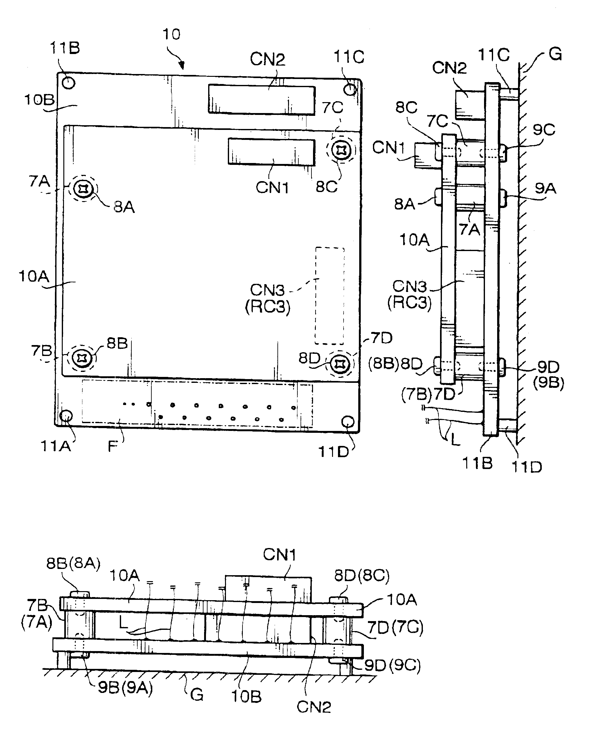
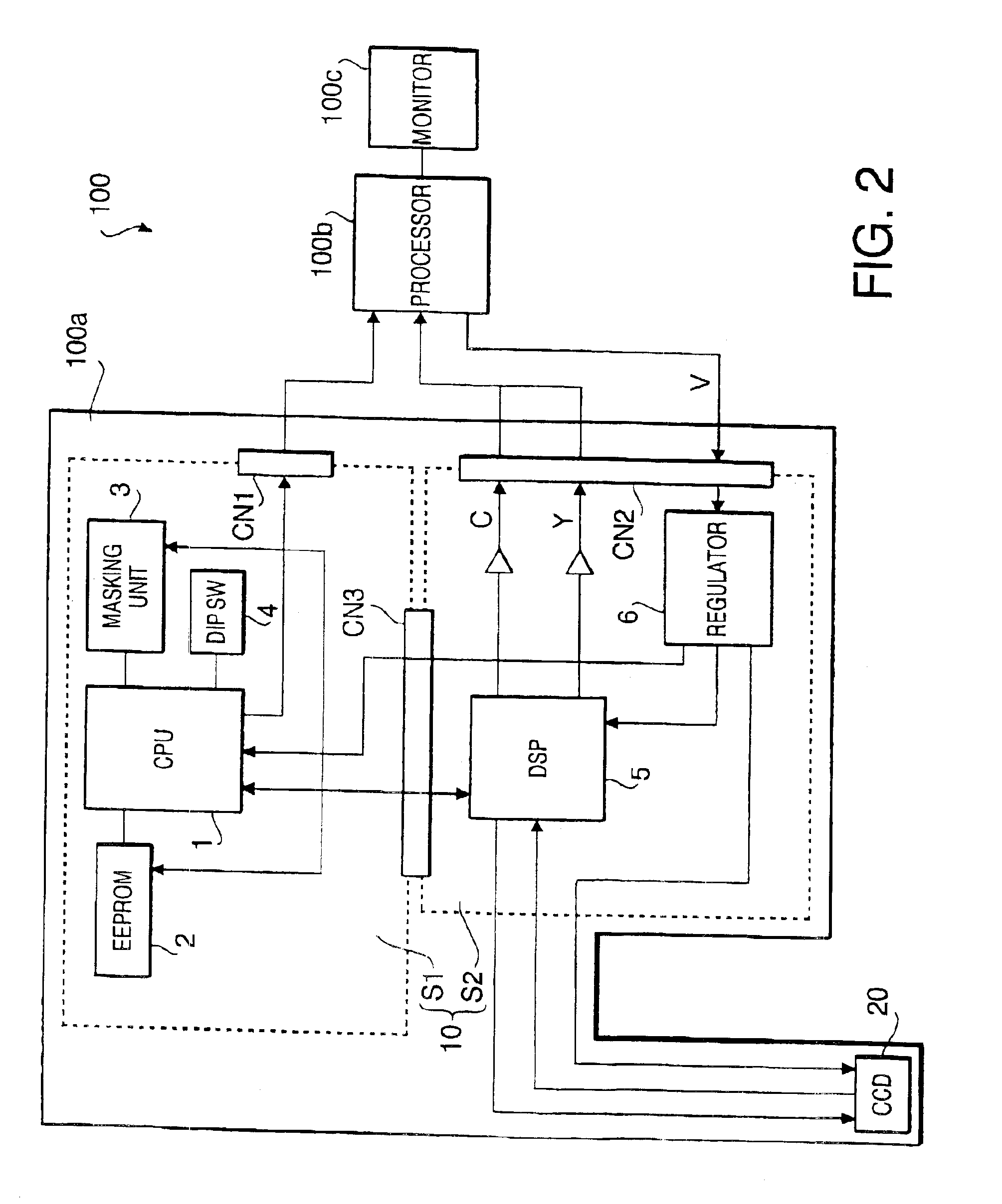
[0021]FIGS. 1A-1C are a plan view, a front view and a side view of the PCB structure, respectively. The PCB structure is employed in an electronic endoscope system 100 (hereinafter, occasionally referred to as endoscope system) according to an embodiment of the invention. FIG. 2 is a block diagram illustrating an electrical configuration of the electronic endoscope system 100.

[0022]The endoscope system 100 includes a scope unit 100a, a processor unit 100b and a monitor 100c. A CCD 20 is provided at a tip end (distal end) of the scope unit 100a.

[0023]Although not shown in the drawings, the processor unit 100b is provided with a power unit for providing electrical power to the connected scope unit 100a, a light source unit for providing light to the scope unit 100a for illuminating an object to be observed, and an image processing unit that processed an image signal captured by the CCD 20 and transmitted from the scope unit.

[0024]The scope unit 100a includes a driving unit 10 which c...


PUM


Abstract

A printed circuit board structure for a scope unit of an electronic endoscope system, which is provided with a first printed circuit board formed with a first circuit section, and a second printed circuit board formed with a second circuit section. The first printed circuit board is piled on the second printed circuit board. The second printed circuit board having an area covered with the first printed circuit board and at least one area which is not covered with the first circuit board. The at least one area is used for electrically connecting the second circuit section with an electrical unit other than the second circuit section.

Description

BACKGROUND OF THE INVENTION[0001]The present invention relates to an electronic endoscope, and more particularly to a PCB (Printed Circuit Board) structure for a scope unit of electronic endoscope.[0002]A medical electronic endoscope is generally provided with a processor having a light source, image processing unit and the like, and an electronic scope (a scope unit) having a portion to be inserted in a human body. The electronic scope has a light guide, which receives the light emitted by the light source from the processor, and illuminates inside the human body, and a CCD (Charge Coupled Device) which captures an image of the illuminated portion.[0003]In such an electronic endoscope, electronic circuits are provided. Typically, an electronic circuit is installed inside a section of the electronic scope in a form of a PCB. In a conventional electronic scope, the PCB is formed of a single substrate having a relatively large area. Generally, such a PCB is provided at a connection se...

Claims


Application Information

Patent Timeline
Patent Type & Authority Patents(United States)
IPC IPC(8): H05K1/14A61B1/05A61B1/04G02B23/24H04N5/225H04N5/335H04N5/357
CPCH05K1/144A61B1/05
Inventor TAKAMI, SATOSHIISHIZUKA, YUKIHIRO
Owner ASAHI KOGAKU KOGYO KK
Why Eureka
Try Eureka