Decoupling capacitor sizing and placement

a capacitor and decoupling technology, applied in the field of deco, can solve the problems of large number of cells, difficult connection between cells, and inability to physically design without the aid of computers

Inactive Publication Date: 2005-05-24
INT BUSINESS MASCH CORP
View PDF5 Cites 43 Cited by
  • Summary
  • Abstract
  • Description
  • Claims
  • Application Information

AI Technical Summary

Benefits of technology

[0012]It is therefore one object of the present invention to provide an improved method of laying out cells in an integrated circuit.
[0013]It is another object of the present invention to provide such a method which utilizes decoupling capacitors in the power grid to reduce noise.
[0014]It is yet another object of the present invention to provide a method and system for improving the placement and sizing of decoupling capacitors between cells in a row-oriented random logic macro structure.

Problems solved by technology

An IC may include a very large number of cells and require complicated connections between the cells.
Due to the large number of components and the details required by the fabrication process, physical design is not practical without the aid of computers.
One problem that has arisen in these modern electronic devices relates to noise in the power grid of the device.
The power grid provides the power and ground signals throughout the chip, and these are among the most important signals to control reliably, since supply voltage variations can lead not only to problems related to spurious transitions in some case (particularly when dynamic logic is used), but also to delay variations and timing unpredictability.
Even if a reliable supply is provided at an input pin of a chip, it can deteriorate significantly within the chip due to imperfections in the conductors that transmit these signals throughout the chip.
Noise in modern electronic circuits is particularly troublesome as it increases the requirements on the noise margins and other circuit parameters.
Noise margins have been greatly reduced in modern designs due to the lowering of supply voltages and the presence of a larger number of potential noise generators.
While the use of decaps is well-known in the art, the prior art designs are so complex that it has heretofore been impossible to optimize the placement and sizing of the decaps in any meaningful way.
Existing methods for adding decoupling capacitance are heuristic and local and are therefore wasteful in chip area.

Method used


Image

  • Decoupling capacitor sizing and placement
  • Decoupling capacitor sizing and placement
  • Decoupling capacitor sizing and placement

Examples


Embodiment Construction

)

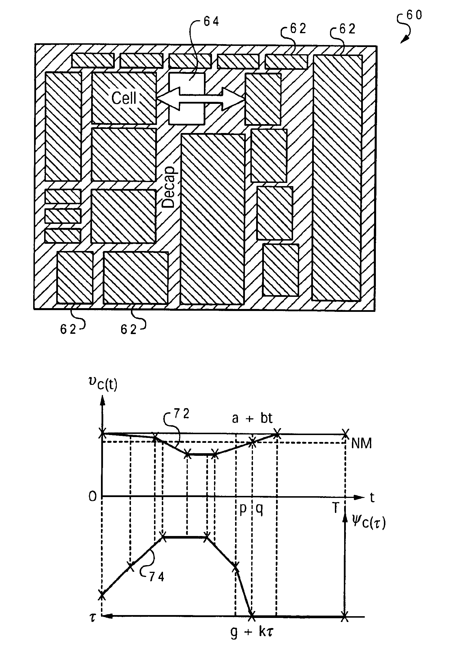
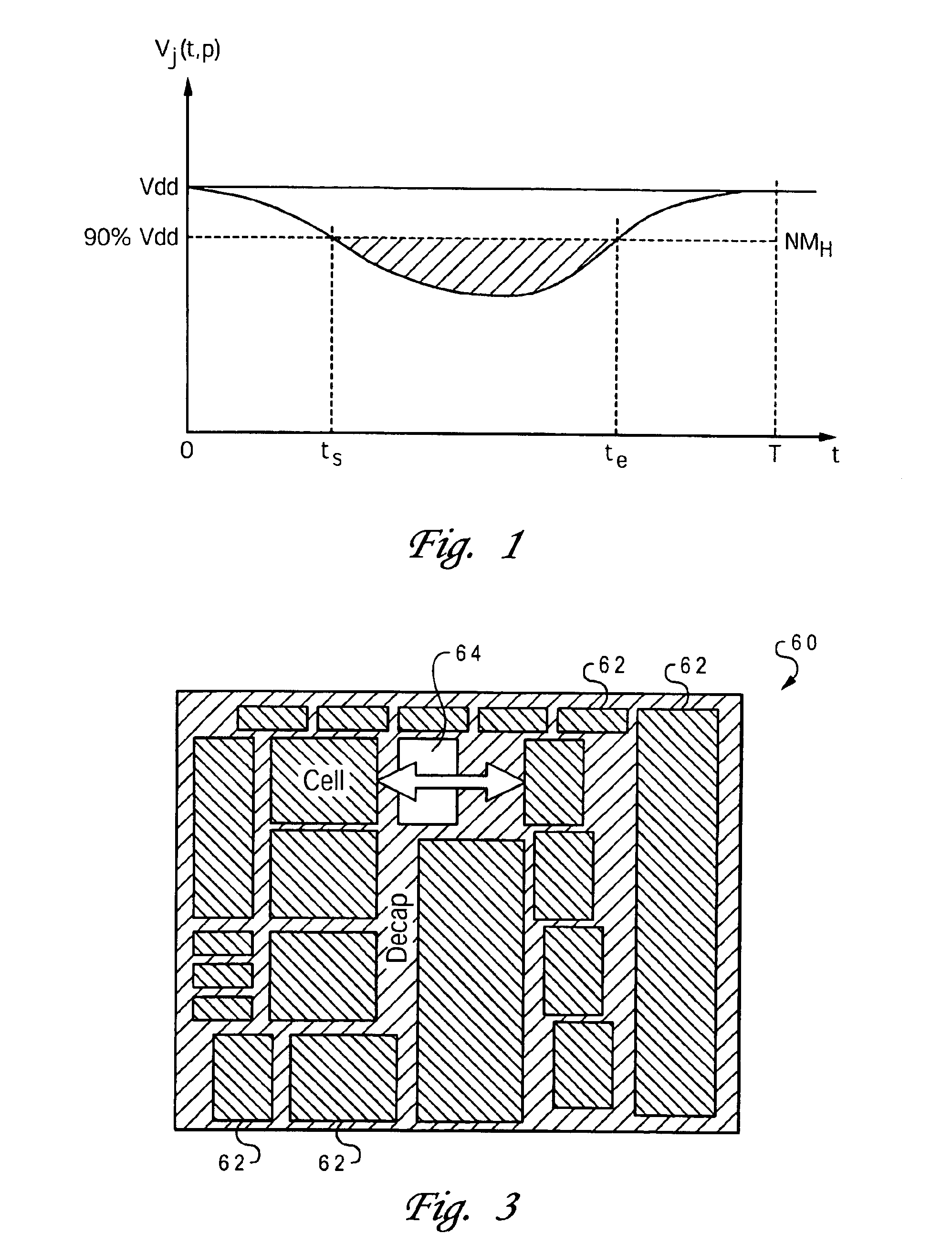
[0026]The present invention is directed to a method and system for automated placement and sizing of decoupling capacitors (decaps) in ASIC-like circuits. In the preferred implementation, an adjoint sensitivity method is applied to calculate the first-order sensitivity of the power grid noise with respect to every decap. As explained further below, a fast convolution technique based on piecewise linear compressions of the original and adjoint waveforms is used to optimize placement. Experimental results show that power grid noise can be significantly reduced after a judicious optimization of decap placement, with little change of the total chip area.

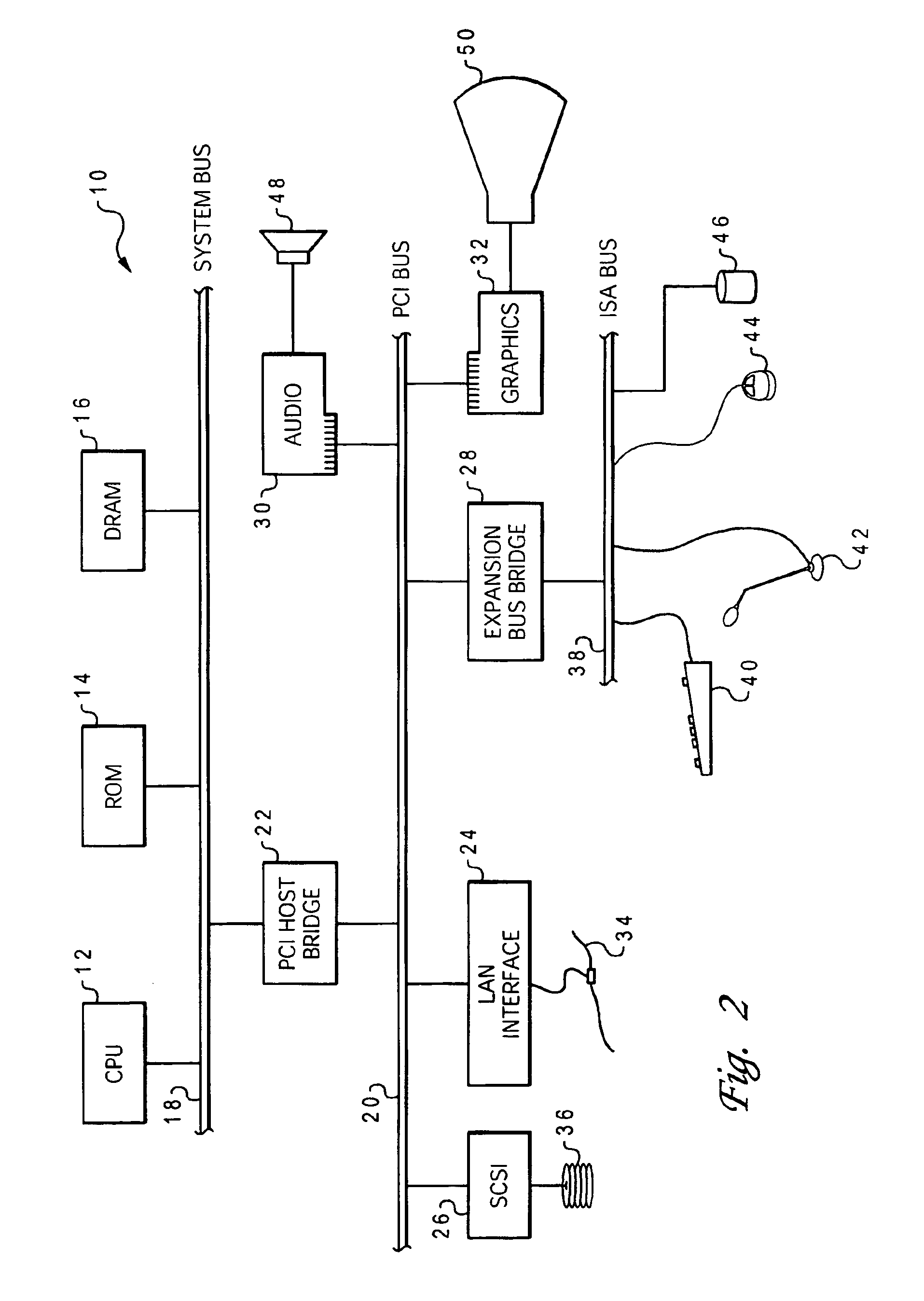
[0027]With reference now to the figures, and in particular with reference to FIG. 2, there is depicted one embodiment 10 of a computer system programmed to carry out computer-aided design of an integrated circuit in accordance with one implementation of the present invention. System 10 includes a central processing unit (CPU) 12 which c...


PUM


Abstract

A method and system for reducing noise in a power grid of an integrated circuit, which optimizes the placement and sizing of decoupling capacitors in the power grid. Logic cells are located in a first layout of the integrated circuit with empty spaces between the adjacent cells, and the placement of the cells is changed to a second layout wherein the size of the empty spaces between the adjacent cells also change. The decoupling capacitors are placed in the empty spaces of the second layout. In the example of a row-oriented cell structure, the empty spaces may be uniformly distributed along each row for the initial layout. An adjoint sensitivity analysis is performed of the sensitivity of a noise function of the integrated circuit with respect to sizes of the empty spaces between adjacent cells, and an original noise waveform is convolved with an adjoint noise waveform. The convolution may use piecewise linear compressions of the original and adjoint noise waveforms. A quadratic programming solver is then used to iteratively determine the sizes of the empty spaces between adjacent cells.

Description

BACKGROUND OF THE INVENTION[0001]1. Field of the Invention[0002]The present invention generally relates to managing noise in a power grid or plane of an electronic device, and more particularly to a method of using decoupling capacitors to reduce noise in an integrated circuit, such as an application specific integrated circuit having rows of random logic macros.[0003]2. Description of the Related Art[0004]Integrated circuits are used for a wide variety of electronic applications, from simple devices such as wristwatches, to the most complex computer systems. A microelectronic integrated circuit (IC) chip can generally be thought of as a collection of logic cells with electrical interconnections between the cells, formed on a semiconductor substrate (e.g., silicon). An IC may include a very large number of cells and require complicated connections between the cells. A cell is a group of one or more circuit elements such as transistors, capacitors, resistors, inductors, and other bas...

Claims


Application Information

Patent Timeline
Patent Type & Authority Patents(United States)
IPC IPC(8): G06F17/50
CPCG06F17/5072G06F30/392
Inventor NASSIF, SANI RICHARDSU, HAIHUA
Owner INT BUSINESS MASCH CORP
Why Eureka
Try Eureka