Retaining ring with wear pad for use in chemical mechanical planarization

a technology of mechanical planarization and wear pad, which is applied in the direction of grinding drive, manufacturing tools, lapping machines, etc., can solve the problems of high cost of cmp equipment operation, abrasion slurry, and subject to polishing action, so as to increase the operating temperature and pressure, reduce the effect of wear

Inactive Publication Date: 2005-05-31
RAYBESTOS POWERTRAIN
View PDF8 Cites 21 Cited by
  • Summary
  • Abstract
  • Description
  • Claims
  • Application Information

AI Technical Summary

Benefits of technology

[0006]It is, therefore, the primary objective of the present invention to provide a retaining ring for use in retaining a wafer during polishing by a CMP apparatus, which has a wear pad associated therewith of such construction, design and material such that it provides improved resistance to wear and / or degradation as compared to currently available products for use in the chemical mechanical planarization (CMP) of semiconductor wafers and similar materials.
[0008]It is yet another objective of the present invention to provide such a retaining ring with a wear pad, with an insulating layer being interposed between the wear pad and the bottom surface of the retaining ring, whereby heat generated during wafer-polishing is better retained in order to elevate the temperature at which wafer-polishing is performed.
[0011]The retaining ring with wear pad of the invention is able to withstand increased operating temperatures and pressures at the polishing surface of the wafer with less wear than would normally be encountered with currently used materials and designs. The ability to operate at increased temperature and pressure can improve the polishing removal rate in some processes such as tungsten, copper and oxide. The flexibility of a manufacturer to use an expanded range of temperature and pressure in CMP processes, combined with a significant reduction in the cost of consumables, provides a significant advantage in the final cost of ownership in the production of multilayer, integrated circuit devices and other products where CMP is utilized in manufacture. Moreover, the retaining-ring wear pad of the present invention may also retrofitted to previously used and worn retaining rings of the prior-art design, thus salvaging the major structural component of the CMP processing apparatus, thereby reducing costs. It is also an integral part of this invention to make the wear pad of the invention replaceable, so as to obviate the necessity of replacement of an entire retaining ring, resulting in considerable cost-savings.

Problems solved by technology

These parts contribute significantly to the high costs of CMP equipment operation.
As such, it is subject to the polishing action of the polishing pad and the abrasive slurry.
Current retaining ring construction materials, although having other desirable properties, do not have good wear resistance.
Replacement of the retaining ring on a regular basis adds substantially to the cost of ownership of the CMP process machinery.
This material seems satisfactory in most regards, but requires frequent replacement as the material wears.

Method used


Image

  • Retaining ring with wear pad for use in chemical mechanical planarization
  • Retaining ring with wear pad for use in chemical mechanical planarization
  • Retaining ring with wear pad for use in chemical mechanical planarization

Examples


first embodiment

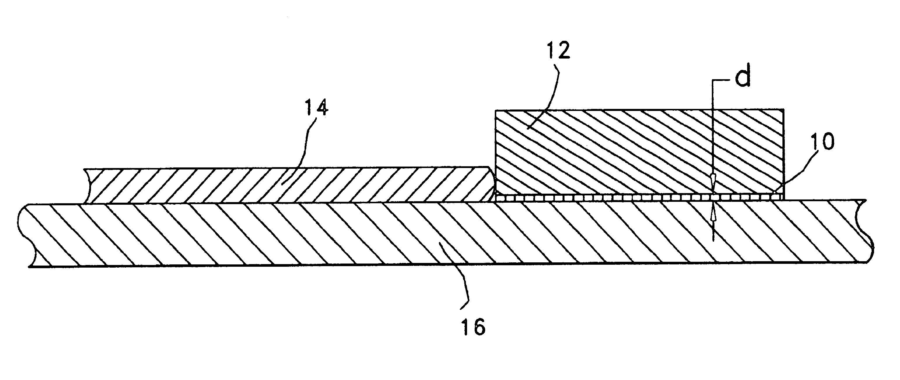
[0020]Referring to the drawings in greater detail, there is shown in FIG. 1 a cross section of the annular retaining ring with wear pad for use in CMP processes, wherein a thin, 0.010 of an inch or less, annular wear pad 10 is adhesively attached to the bottom of annular retaining ring 12, which retaining ring is constructed of a thermoplastic material, such as PPS. A semiconductor wafer 14 to be polished by a polishing head of a CMP apparatus is shown abutting the inside annular surface of the retaining ring 12 and retained thereby. The bottom surface of the wafer 14 and the annular wear pad 10 are in contact with polishing pad 16 of a conventional polishing head assembly described hereinbelow with reference to FIG. 2. The embodiment of FIG. 1 significantly reduces retaining-ring wear by replacing about 0.010 inches or less at the contact surface of the retaining ring with about 0.010 inches or less of the thick wear pad 10 of material bonded to the PPS of the retaining ring. While...

second embodiment

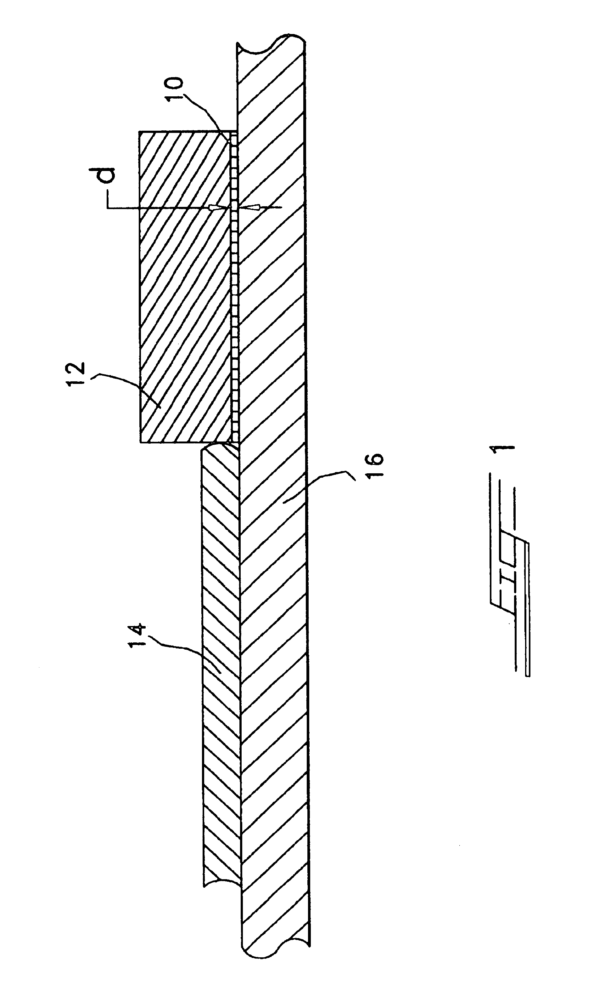
[0028]FIG. 3 is a cross section of a second embodiment, wherein a relatively thick annular wear pad 20 is inserted into a bottom, outer annular, cutout portion 22 of retaining ring 22, such that the wear pad 20 is in contact with the polishing pad 16. The portion of the retaining ring that contacts the wafer 14 at its interior annular surface has a relieved section 24 at its the bottom thereof, so that retaining ring proper does not contact the polishing pad 16. The relieved section 24 extends outwardly from the interior annular surface toward the exterior, or outer, annular surface of the retaining ring, such that it extends until reaching the interior annular surface of the wear pad 20. Preferably, but not required, the relieved section 24 has a depth “d”, as measured from the top toward the bottom of the retaining ring, that is less than the depth, or height, of the wear pad 20, as seen in FIG. 3. The wear pad 20 protrudes about 0.010 inches or less beyond this relieved section 2...

third embodiment

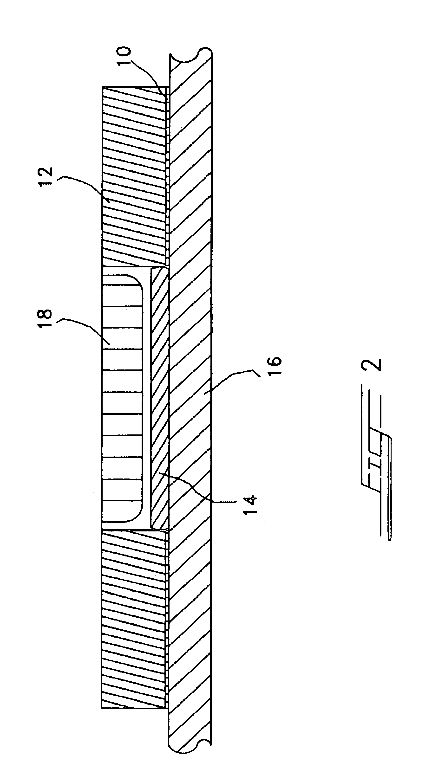
[0029]FIG. 4 is a cross section of a third embodiment, wherein the annular retaining ring 32 is comprised of wear-pad material, thus effectively making the retaining ring 32 one large wear pad itself. The retaining ring 32 is formed with a bottom, interior annular cutout section or portion 34, in which is adhered, or otherwise formed, a relatively small, interior, annular or ring-shaped force-absorbing insert 36, of a suitable thermoplastic material, such as PPS, in order to act as a bumper against the wafer 14 during polishing. There is a gap “d” between the bottom surface of the annular, force-absorbing insert 36 and the bottom surface of the retaining ring, so that the force-absorbing ring 36 does not contact the polishing pad 16. The bottom surface of the annular retaining ring / wear pad combination protrudes preferably about 0.010 inches or less below the insert 36, so as to effectively provide a wear-pad section that resists the heat and abrasion of the polishing operation.


PUM


Abstract

A novel retaining ring having a wear pad of such construction, design and material such that it provides improved resistance to wear and / or degradation as compared to currently available products for use in the chemical mechanical planarization (CMP) of semiconductor wafers and similar materials. The retaining ring with wear pad of the invention is able to withstand increased operating temperatures and pressures at the polishing surface of the wafer with less wear than would normally be encountered with currently used materials and designs. The ability to operate at increased temperature and pressure can accelerate the rate of removal of material from a semiconductor wafer in some processes. The flexibility of a manufacturer to use an expanded range of temperature and pressure in CMP processes, combined with a significant reduction in the cost of consumables, provides a significant advantage in the final cost of ownership in the production of multilayer, integrated circuit devices and other products where CMP is utilized in manufacture. Moreover, the retaining with wear pad of the present invention may also retrofitted to previously used and worn retaining rings of the prior-art design, thus salvaging the major structural component of the CMP processing apparatus, thereby reducing costs. It is also an integral part of this invention to make the consumable component of the new design replaceable, so as to make replacement of this part less costly when such replacement finally does become necessary.

Description

CROSS REFERENCE TO RELATED APPLICATION[0001]Priority of provisional application Ser. No. 60 / 295,472, filed on Jun. 1, 2001, is hereby claimed.BACKGROUND OF THE INVENTION[0002]Enabling technology for the manufacture of multiple layer integrated circuit devices has been chemical mechanical planarization (CMP). In this process, each layer of wiring devices or of insulating material is polished flat (planarized) prior to deposition of the next layer. CMP facilitates the construction of multi-layer integrated circuit devices by reducing irregularities in surface topography to an acceptable level, to thus prevent defects such as short circuits or open circuits as the layers are built up.[0003]The machinery to perform CMP has become highly sophisticated and efficient, with equipment costing millions of dollars. Nevertheless, there are some components of this equipment that require frequent replacement during the polishing operation, and are classed as consumables. These parts contribute si...

Claims


Application Information

Patent Timeline
Patent Type & Authority Patents(United States)
IPC IPC(8): B24B37/04B24B37/32
CPCB24B37/32
Inventor COOPER, RICHARD D.FATHAUER, PAULMROCZEK-PETROSKI, ANGELAPERRY, DAVIDMACEY, JAMES P.
Owner RAYBESTOS POWERTRAIN
Why Eureka
Try Eureka