Reusable ceramic-comprising component which includes a scrificial surface layer

a ceramic surface and scrificial surface technology, applied in the direction of metallic material coating process, diaphragm, chemical vapor deposition coating, etc., can solve the problems of high resistance of tantalum to chemical etchants and is not easily removed by conventional means, so as to achieve effective roughening of ceramic surfaces, reduce microcracking and other damage, and reduce the effect of microcracking

Inactive Publication Date: 2005-05-31
APPLIED MATERIALS INC
View PDF7 Cites 17 Cited by
  • Summary
  • Abstract
  • Description
  • Claims
  • Application Information

AI Technical Summary

Benefits of technology

[0011]We have discovered a method of roughening a ceramic surface in which mechanical interlocks are formed in the ceramic surface (such as an aluminum oxide surface) by chemical etching, thermal etching, or using a laser micromachining process. The method of the invention results in an effectively roughened ceramic surface which provides good adherence to an overlying sacrificial layer (such as aluminum), while minimizing microcracking and other damage to the ceramic surface. Because there is essentially no chemical bonding between the ceramic and an overlying, typically metal sacrificial layer, the method of the invention functions by enlarging the contact area between the ceramic surface and the sacrificial layer, and mechanically locking the sacrificial layer to the ceramic surface.

Problems solved by technology

However, tantalum is highly resistant to chemical etchants and is not easily removed by conventional means.
It is therefore believed that surface properties of the ceramic are a major contributing factor in the observed failures.

Method used


Image

  • Reusable ceramic-comprising component which includes a scrificial surface layer
  • Reusable ceramic-comprising component which includes a scrificial surface layer
  • Reusable ceramic-comprising component which includes a scrificial surface layer

Examples


Embodiment Construction

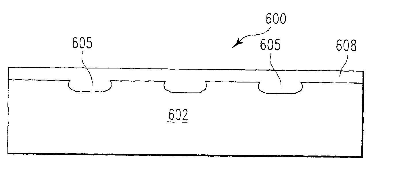
[0020]Disclosed herein is a method of roughening a ceramic surface by forming mechanical interlocks in the ceramic surface by chemical etching, thermal etching, or using a laser micromachining process. The method is applicable for promoting adherence of an overlying layer to an underlying ceramic surface for use in semiconductor processing chambers. To illustrate the invention, applicants describe the invention with reference to use in a physical vapor deposition (PVD) chamber. The ceramic surface has mechanical interlocks formed therein by chemical etching, thermal etching, or laser micromachining. Exemplary processing conditions for performing the method of the invention are set forth below.

[0021]As a preface to the detailed description, it should be noted that, as used in this specification and the appended claims, the singular forms “a”, “an”, and “the” include plural referents, unless the context clearly dictates otherwise.

I. Method of Roughening a Ceramic Surface

[0022]The pres...


PUM

PropertyMeasurementUnit
thicknessaaaaaaaaaa
thicknessaaaaaaaaaa
angleaaaaaaaaaa

Abstract

Disclosed herein is a method of roughening a ceramic surface by forming mechanical interlocks in the ceramic surface by a chemical etching process, a thermal etching process, or a laser micromachining process. Also disclosed herein are components for use in semiconductor processing chambers (in particular, a deposition ring for use in a PVD chamber) which have at least one ceramic surface having mechanical interlocks formed therein by chemical etching, thermal etching, or laser micromachining. Ceramic surfaces which have been roughened according to the chemical etching, thermal etching, or laser micromachining process of the invention are less brittle and damaged than ceramic surfaces which are roughened using conventional grit blasting techniques. The method of the invention results in a roughened ceramic surface which provides good adherence to an overlying sacrificial layer (such as aluminum).

Description

BACKGROUND OF THE INVENTION[0001]1. Field of the Invention[0002]The present invention pertains to methods of roughening a ceramic surface in order to promote adherence of a material applied over the ceramic. The invention also pertains to components for use in semiconductor processing equipment which include roughened ceramic surfaces.[0003]2. Brief Description of the Background Art[0004]In semiconductor device manufacturing, physical vapor deposition (PVD) is a process which is frequently used to deposit a layer of material onto a substrate. FIG. 1 shows a cross-sectional schematic of a PVD processing chamber 100. During a PVD process, a plasma (such as an argon plasma) is used to sputter material (such as copper or tantalum) from a target 102 onto the surface of a semiconductor substrate 104 (typically a silicon wafer), which sits atop an electrostatic chuck 106. A deposition ring 108 is positioned over the exposed upper surface of the chuck 106 which extends beyond the outer edge...

Claims


Application Information

Patent Timeline
Patent Type & Authority Patents(United States)
IPC IPC(8): B23K26/40B23K26/00C04B41/88C04B41/00C04B41/45C04B41/91C04B41/52C04B41/51C04B41/53C04B41/80C04B41/89C23C14/56H01L21/203H05K3/00H05K3/38
CPCB23K26/408C04B41/0072C23C14/564C04B41/91C04B41/89C04B41/88C04B41/80C04B41/5353C04B41/52C04B41/5155C04B41/51C04B41/009C04B41/53C04B41/5133C04B35/10C04B35/00B23K26/40B23K2103/52
Inventor WELDON, EDWIN CHARLESHE, YONGXIANGWANG, HONGSTOW, CLIFFORD C.
Owner APPLIED MATERIALS INC
Why Eureka
Try Eureka